Vertically-integrated double-gate MOSFET structure and preparation method therefor

A technology of metal gate and gate dielectric layer, which is used in semiconductor/solid-state device manufacturing, semiconductor devices, electrical components, etc. Small parasitic capacitance, the effect of shortening the length

Active Publication Date: 2017-01-04
INST OF MICROELECTRONICS CHINESE ACAD OF SCI
View PDF3 Cites 5 Cited by
  • Summary
  • Abstract
  • Description
  • Claims
  • Application Information

AI Technical Summary

Problems solved by technology

[0005] In order to solve the problems of short channel effect, source-drain punch-through, doping fluctuation, difficulty in improving device integration, and metal interconnection delay in the traditional MOSFET device structure during the process of decreasing device gate length, the present invention discloses a vertical Integrated double-gate MOSFET structure and its preparation method

Method used


Image

  • Vertically-integrated double-gate MOSFET structure and preparation method therefor
  • Vertically-integrated double-gate MOSFET structure and preparation method therefor
  • Vertically-integrated double-gate MOSFET structure and preparation method therefor

Examples


preparation example Construction

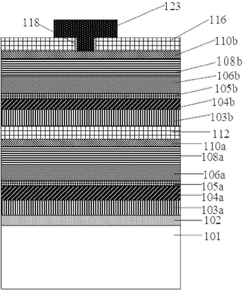
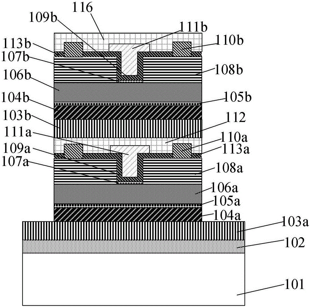
[0067] The invention also discloses a method for preparing a vertically integrated double-gate MOSFET structure, which includes the following steps:

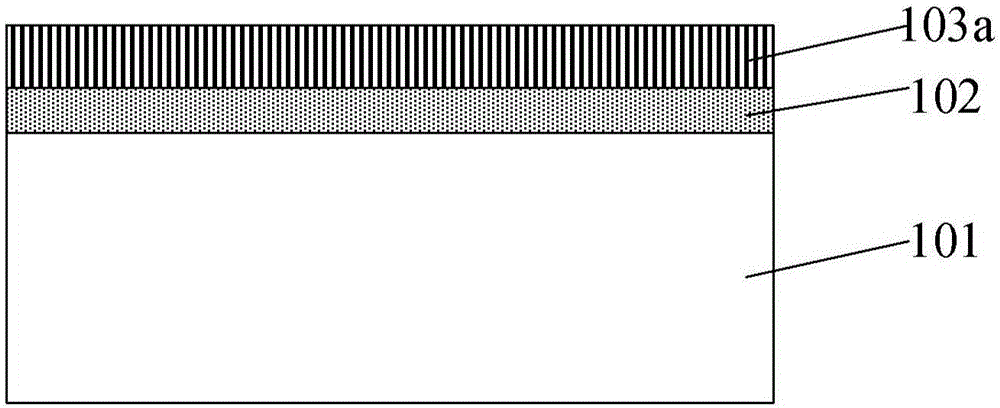
[0068] Step 1. Depositing a first gate metal layer on the isolation layer formed by the substrate to form a first bonding sheet;

[0069] Step 2, forming a second bonding sheet and a third bonding sheet;

[0070] Step 3, bonding the first bonding sheet and the second bonding sheet together;

[0071] Step 4, bonding the second bonding sheet and the third bonding sheet together;

[0072] Step 5, respectively forming the first metal gate electrode 117, the second metal gate electrode 119, the third metal gate electrode 120, the fourth metal gate electrode 121, the first metal source-drain electrode 122 and the second metal source-drain electrode 123;

[0073] Step 6, lead out the source-drain metal and the gate metal to form the first metal source-drain electrode 122, the second metal source-drain electrode 123, the first metal g...


PUM


Abstract

The invention discloses a vertically-integrated double-gate MOSFET structure and a preparation method therefor. Compared with a conventional planar MOSFET structure, the vertically-integrated double-gate MOSFET structure adopts an III-V group semiconductor material with high electron mobility / hole mobility as a channel material; due to the adopted double-gate structure, the gate control capability of an MOSFET device is effectively improved, and influence from a short channel effect and the like is reduced; an NMOS and a PMOS are integrated in a vertical direction, so that the integration degree of devices on a unit wafer area is improved; and vertical through holes are adopted to realize interconnection of the devices in the vertical direction, so that the length of an interconnecting lead is effectively shortened while the operation speed of the devices is improved. The vertically-integrated double-gate MOSFET structure provided by the invention has an important application value in a post-Moore era CMOS integration technology and a high-performance III-V group semiconductor device.

Description

technical field [0001] The invention relates to the technical field of semiconductor integration, in particular to a vertically integrated double-gate MOSFET structure and a preparation method thereof. Background technique [0002] As the core and foundation of the information industry, semiconductor technology is regarded as an important symbol to measure a country's scientific and technological progress and comprehensive national strength. With the continuous scaling down of the feature size of MOS devices and the continuous improvement of integrated circuit integration, it has become more and more difficult to develop according to Moore's Law, which doubles every 18 months. However, when the feature size reaches 90 nanometers, traditional silicon-based CMOS devices are facing more and more problems. The introduction of new structures and new materials has become one of the solutions in the post-Moore era. [0003] In the process of decreasing the gate length of the tradi...

Claims


Application Information

Patent Timeline
Patent Type & Authority Applications(China)
IPC IPC(8): H01L29/423H01L29/78H01L21/336H01L27/02
CPCH01L27/0207H01L29/42356H01L29/66484H01L29/7831
Inventor 王盛凯李跃刘洪刚孙兵常虎东龚著靖
Owner INST OF MICROELECTRONICS CHINESE ACAD OF SCI
Why Eureka
Try Eureka