Check patentability & draft patents in minutes with Patsnap Eureka AI!

Manufacturing method of flash memory structure

A manufacturing method and technology of flash memory, which is applied in semiconductor/solid-state device manufacturing, electrical components, electric solid-state devices, etc., can solve the problems that the electrical performance and yield rate of flash memory structure need to be improved, and achieve the effect of improving electrical performance and yield rate

Active Publication Date: 2016-03-23
SHANGHAI HUAHONG GRACE SEMICON MFG CORP
View PDF2 Cites 11 Cited by
  • Summary
  • Abstract
  • Description
  • Claims
  • Application Information

AI Technical Summary

Problems solved by technology

[0004] However, the electrical performance and yield of the flash memory structure in the prior art need to be improved

Method used


Image

  • Manufacturing method of flash memory structure
  • Manufacturing method of flash memory structure
  • Manufacturing method of flash memory structure

Examples


Embodiment Construction

[0012] It can be seen from the background art that the electrical performance and yield of the flash memory structure formed in the prior art need to be improved.

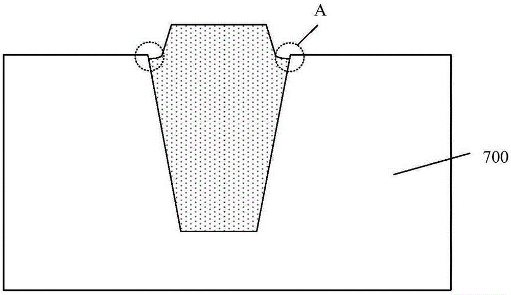
[0013] refer to figure 1 and figure 2 , shows a schematic structural diagram of a flash memory structure in the prior art. Analyze the reasons for this:

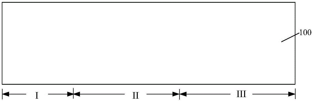
[0014] refer to figure 1 , figure 1 (a) is a structural schematic diagram after forming the first isolation structure (not marked), the second isolation structure 740 and the third isolation structure 720, figure 1 (b) is a schematic structural view after forming the sidewall layer 730 in the third region through subsequent process steps, and figure 1 (a) and figure 1 (b) is a schematic diagram of the cross-sectional structure in different directions. The substrate 700 includes a first region I, a second region II and a third region III.

[0015] The first region I is a memory cell region, the third region III substrate 700 is a peripheral device region,...


PUM


Abstract

A manufacturing method of a flash memory structure comprises the steps of providing a substrate of a first region; forming a floating gate layer and a hard mask layer on the substrate in sequence; forming trenches, comprising a first trench in the first region, in the hard mask layer, the floating gate layer and the substrate; filling the first trench with an isolation material; using the hard mask layer as a stopping layer, grinding to remove the isolation material higher than the hard mask layer and forming a first initial isolation structure with a first thickness value in the first trench; according to a difference value between a target thickness value of the first initial isolation structure and the first thickness value, performing dynamic adjusting etching to remove a part of the thickness of the first initial isolation structure to form a first isolation structure. The dynamic adjusting etching is performed according to the difference value between the target thickness value and the first thickness value, a part of the thickness of the first initial isolation structure is removed to form the first isolation structure, the difference value is reduced, the problem that corners of the substrate at two sides of the first isolation structure are exposed is solved and electrical performances of the flash memory structure are improved.

Description

technical field [0001] The invention relates to the field of semiconductors, in particular to a method for manufacturing a flash memory structure. Background technique [0002] In the current semiconductor industry, integrated circuit products can be mainly divided into three types: analog circuits, digital circuits, and digital / analog hybrid circuits. Among them, memory devices are an important type of digital circuits. Among storage devices, the development of flash memory (Flash Memory, referred to as flash memory) is particularly rapid in recent years. The main feature of flash memory is that it can keep stored information for a long time without power on; and it has the advantages of high integration, fast access speed, easy erasing and rewriting, etc., so it has been widely used in many fields such as microcomputer and automatic control. a wide range of applications. [0003] The flash memory structure is different from the conventional MOS transistor structure. The...

Claims


Application Information

Patent Timeline
IPC IPC(8): H01L21/8247H01L21/762
CPCH01L21/762H01L21/76224H10B41/00
Inventor 曹子贵
Owner SHANGHAI HUAHONG GRACE SEMICON MFG CORP
Features
  • R&D
  • Intellectual Property
  • Life Sciences
  • Materials
  • Tech Scout
  • Unparalleled Data Quality
  • Higher Quality Content
  • 60% Fewer Hallucinations
Learn More