Array substrate and manufacturing method thereof as well as display device

A technology of an array substrate and a manufacturing method, which is applied in the display field, can solve the problems of many patterning processes, increase the manufacturing cost of the array substrate, restrict the production capacity, etc., and achieve the effects of improving production efficiency, reducing the number of patterning processes, and reducing manufacturing costs.

Active Publication Date: 2016-03-30
BOE TECH GRP CO LTD
View PDF3 Cites 8 Cited by
  • Summary
  • Abstract
  • Description
  • Claims
  • Application Information

AI Technical Summary

Problems solved by technology

[0004] At present, Oxide (metal oxide semiconductor) technology is developing rapidly, and metal oxide semiconductor has become an ideal material for the active layer of TFT array substrates due to its simple preparation process and excellent optoelectronic properties; in addition, due to the high PPI (pixel density) requirements

Method used


Image

  • Array substrate and manufacturing method thereof as well as display device
  • Array substrate and manufacturing method thereof as well as display device
  • Array substrate and manufacturing method thereof as well as display device

Examples


Example Embodiment

[0059] Embodiment one

[0060] This embodiment provides a method for manufacturing an array substrate, and the method includes:

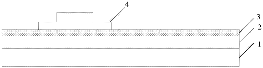
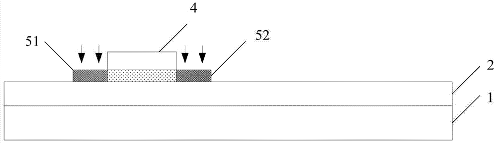
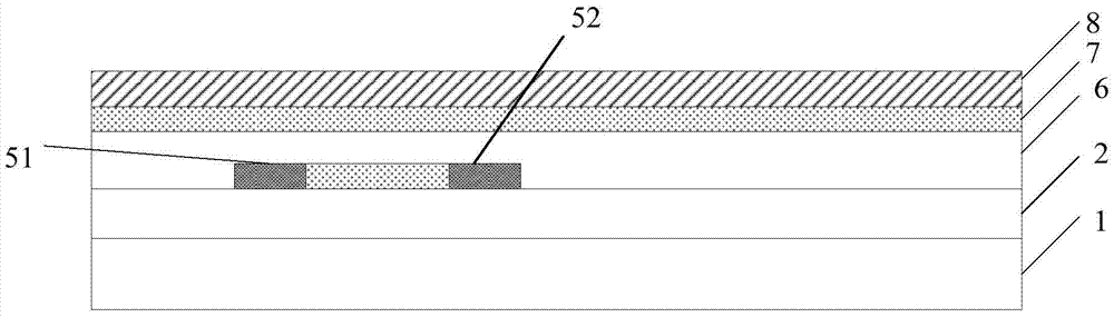
[0061] A gate electrode, a gate line, a data line, a source electrode and a drain electrode are formed on the gate insulating layer through a patterning process, so that the gate electrode, the gate line, the data line, the source electrode and the drain electrode are arranged in the same layer and the same material.

[0062] In this embodiment, the gate electrodes, gate lines, data lines, source electrodes, and drain electrodes are formed by one patterning process, and the gate electrodes, gate lines, data lines, source electrodes, and drain electrodes are located on the same layer. The times of patterning process can be increased, production efficiency can be improved, and production cost can be reduced; on the other hand, there is no overlapping area between the gate electrode, source electrode, and drain electrode, which can effectively reduce t...

Example Embodiment

[0086] Embodiment two

[0087] This embodiment also provides an array substrate manufactured by the above manufacturing method, wherein the gate electrode, gate line, data line, source electrode and drain electrode of the array substrate are arranged in the same layer and with the same material.

[0088] In this embodiment, the gate electrode, gate line, data line, source electrode, and drain electrode are located on the same layer, and can be formed by the same patterning process. On the one hand, it can reduce the number of patterning processes when preparing the array substrate, improve production efficiency, and reduce production Cost; on the other hand, there is no overlapping area between the gate electrode and the source electrode and the drain electrode, which can effectively reduce the coupling capacitance between the source electrode, the drain electrode and the gate electrode of the array substrate, thereby reducing the power consumption of the array substrate.

[0...

Example Embodiment

[0099] Embodiment three

[0100] An embodiment of the present invention also provides a display device, including the above-mentioned array substrate. The display device may be any product or component with a display function such as an OLED panel, a mobile phone, a tablet computer, a television set, a monitor, a notebook computer, a digital photo frame, a navigator, and the like.


PUM


Abstract

The present invention provides an array substrate and a manufacturing method thereof as well as a display device, and belongs to the technical field of display. The manufacturing method of the array substrate comprises the following steps: forming a gate electrode, a gate line, a data line, a source electrode and a drain electrode on an insulation layer through a one-step patterning process; and installing the gate electrode, the gate line, the data line, the source electrode and the drain electrode in the same layer by using the same material. The technical solution of the present invention can reduce the number of times of patterning process when the array substrate is prepared, increase the production efficiency, reduce the manufacturing cost, and can also reduce a coupling capacitance among the source electrode, the drain electrode and the grate electrode of the array substrate, thereby reducing the power consumption of the array substrate.

Description

technical field [0001] The present invention relates to the field of display technology, in particular to an array substrate, a manufacturing method thereof, and a display device. Background technique [0002] With the progress of TFT (ThinFilmTransistor, thin film transistor) industry and the improvement of technology, ADS (ADvancedSuperDimensionSwitch, Advanced Super Dimension Switch) wide viewing angle technology has been applied to more and more products, including mobile phones, digital cameras, tablet computers , notebook computers, and LCD TVs, etc., its excellent display characteristics have been praised by more and more users, and its market competitiveness is very strong. [0003] ADS technology is to form a multi-dimensional electric field through the electric field generated by the edge of the slit electrode in the same plane and the electric field generated between the slit electrode layer and the plate electrode layer, so that all oriented liquid crystal molecu...

Claims


Application Information

Patent Timeline
IPC IPC(8): H01L21/77H01L21/28H01L27/12G02F1/1362
CPCG02F1/1362H01L21/28H01L21/77H01L27/12
Inventor 卢鑫泓王珂齐峰胡合合
Owner BOE TECH GRP CO LTD
Why Eureka
Try Eureka