Wafer cutting method
A cutting method and wafer technology, which can be used in electrical components, fine working devices, semiconductor/solid-state device manufacturing, etc., can solve problems such as chipping at the top edge of deep reactive ion etching trenches
- Summary
- Abstract
- Description
- Claims
- Application Information
AI Technical Summary
Problems solved by technology
Method used
Image
Examples
Embodiment 1
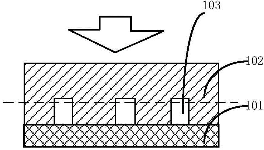
[0043] Current methods for dicing wafers with high-aspect-ratio trenches are figure 1 As shown, a semiconductor substrate 102 is firstly provided, and several trenches 103 with a high aspect ratio are formed in the semiconductor substrate 102 by means of deep reactive ion etching (DRIE), and then the front surface of the semiconductor substrate is bonded. Put a layer of tape (tape) 101 on it, and reverse the semiconductor substrate 102 for back grinding, so as to expose the trench 103 with high aspect ratio, so as to achieve the purpose of cutting (Dicing), such as figure 1 shown.
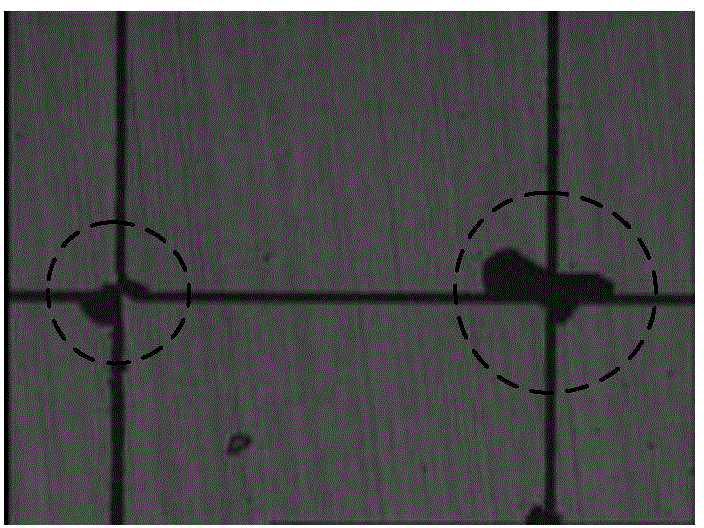
[0044] In DRIE cutting, the cutting and pressure of the grinding wheel on the wafer when approaching the groove 103 and the grinding trench (grinding trench) can easily cause severe chipping (chipping) on the top of the groove 103, such as figure 2 shown.
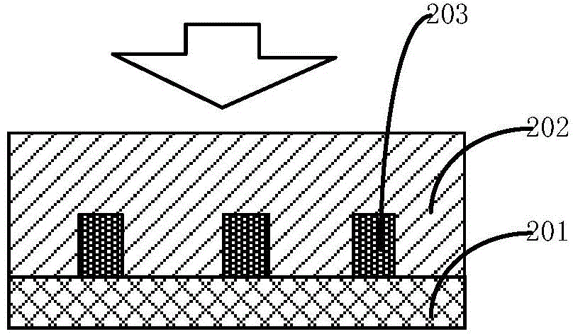
[0045] In order to solve the problems existing in the prior art, the present invention provides a new wafer cutting method, the following ...
PUM
 Abstract
Description
Claims
Application Information


