

High-K metal gate CMOS device and forming method thereof
A metal gate and device technology, applied in the direction of semiconductor devices, semiconductor/solid-state device manufacturing, electrical components, etc., can solve the problem of no barrier layer, affecting the work function value of the PMOS work function metal layer 15, and the small size of the second gate opening 112 and other issues to achieve the effect of eliminating the impact
- Summary
- Abstract
- Description
- Claims
- Application Information
AI Technical Summary
Problems solved by technology
Method used
Image

Examples
no. 1 example
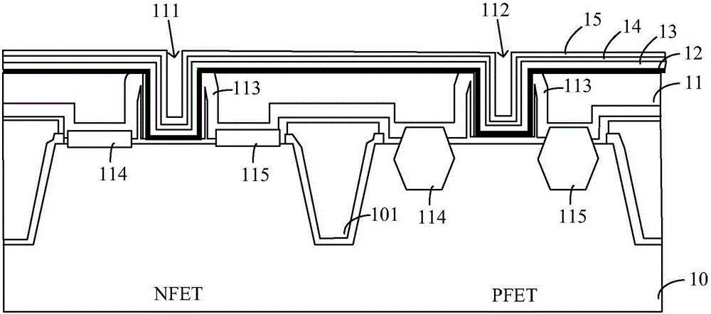
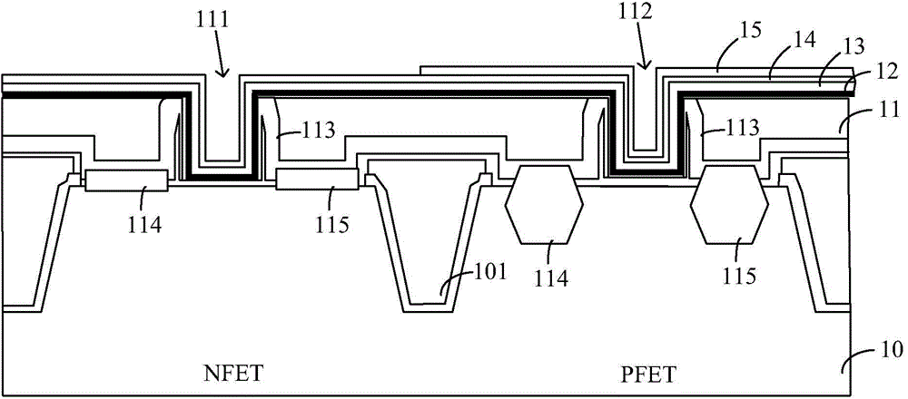
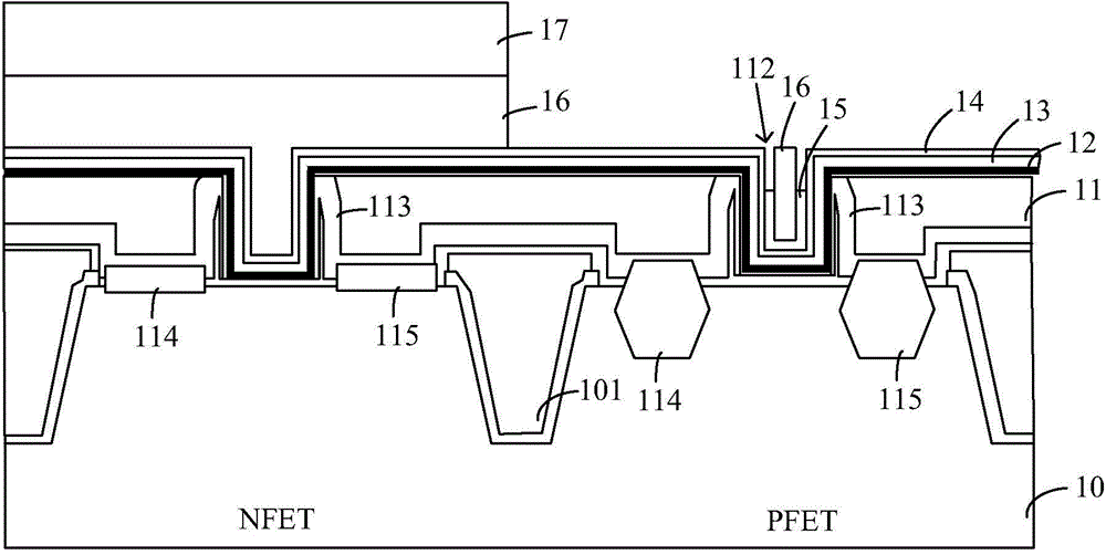
[0066] refer to Figure 7 , a semiconductor substrate 20 is provided, and the semiconductor substrate 20 includes a juxtaposed NMOS region and a PMOS region. The semiconductor substrate 20 may be, for example, a silicon substrate, or other suitable substrates used in semiconductor processes. An isolation structure 201 may be formed in the semiconductor substrate 20 , such as a shallow trench isolation (STI) or the like.
[0067] A dielectric layer 21 is formed on the semiconductor substrate 20. The dielectric layer 21 has a first gate opening 211 in the NMOS region and a second gate opening 212 in the PMOS region. Spacers 213 may be formed in the dielectric layer 11 around the first gate opening 211 and the second gate opening 212 . An active region 214 and a drain region 215 may be formed in the semiconductor substrate 10 on both sides of the first gate opening 211 and the second gate opening 212 .
[0068] The formation process of the first gate opening 211 and the second...
no. 2 example
[0086] The steps of the second example are the same as those of the aforementioned first example Figure 7 to Figure 11 The steps shown are all the same, the difference is that the process after the formation of the PMOS work function metal layer 28 is slightly different.
[0087] refer to Figure 13 , in the PMOS work function metal layer 28 of the first thickness (see Figure 12 ) is formed, the same material can be deposited continuously to increase its thickness, that is, to form a PMOS work function metal layer 28' with a preset second thickness. As the thickness of the PMOS work function metal layer 28' increases, its equivalent work function value also increases. In addition, the thicker PMOS work function metal layer 28' also helps prevent Al from diffusing into the PMOS work function metal layer 28'.
[0088] After that, metal material 30 is filled in the first gate opening and the second gate opening to form gate electrodes. The formation process of the gate elec...
PUM
 Abstract
Description
Claims
Application Information