Die bonding method for flip LED chips

An LED chip, flip-chip technology, applied in electrical components, circuits, semiconductor devices, etc., can solve problems such as unfavorable heat transfer of LED chips, affecting LED light output, and chips prone to skew, achieving small thickness and increasing LED light output. The effect of high efficiency and heat dissipation efficiency

Inactive Publication Date: 2016-03-30
GUANGDONG RAYTON INTELLIGENT OPTO CO LTD
View PDF5 Cites 1 Cited by
  • Summary
  • Abstract
  • Description
  • Claims
  • Application Information

AI Technical Summary

Problems solved by technology

Due to the close distance between the positive and negative electrodes at the bottom of the chip, it is easy to produce a short circuit during production; and the solder paste has a certain fluidity when it melts, which makes the chip prone to skewing; the high-temperature metal is oxidized and blackened, and the metal silver and sulfur produce black silver sulfide. Seriously affect the light output of the LED; there are inevitably voids when the solder paste is cured. If the number of voids is more, the possibility of product soldering is greater
And the metal particle size of solder paste or silver glue as a conductive material exceeds 10um, which makes the gap between the LED chip and the wire about 25-50um, which is extremely unfavorable for the heat transfer generated by the LED chip

Method used


Image

  • Die bonding method for flip LED chips
  • Die bonding method for flip LED chips
  • Die bonding method for flip LED chips

Examples


Embodiment Construction

[0027] The present invention will be further described below in conjunction with the accompanying drawings of the specification.

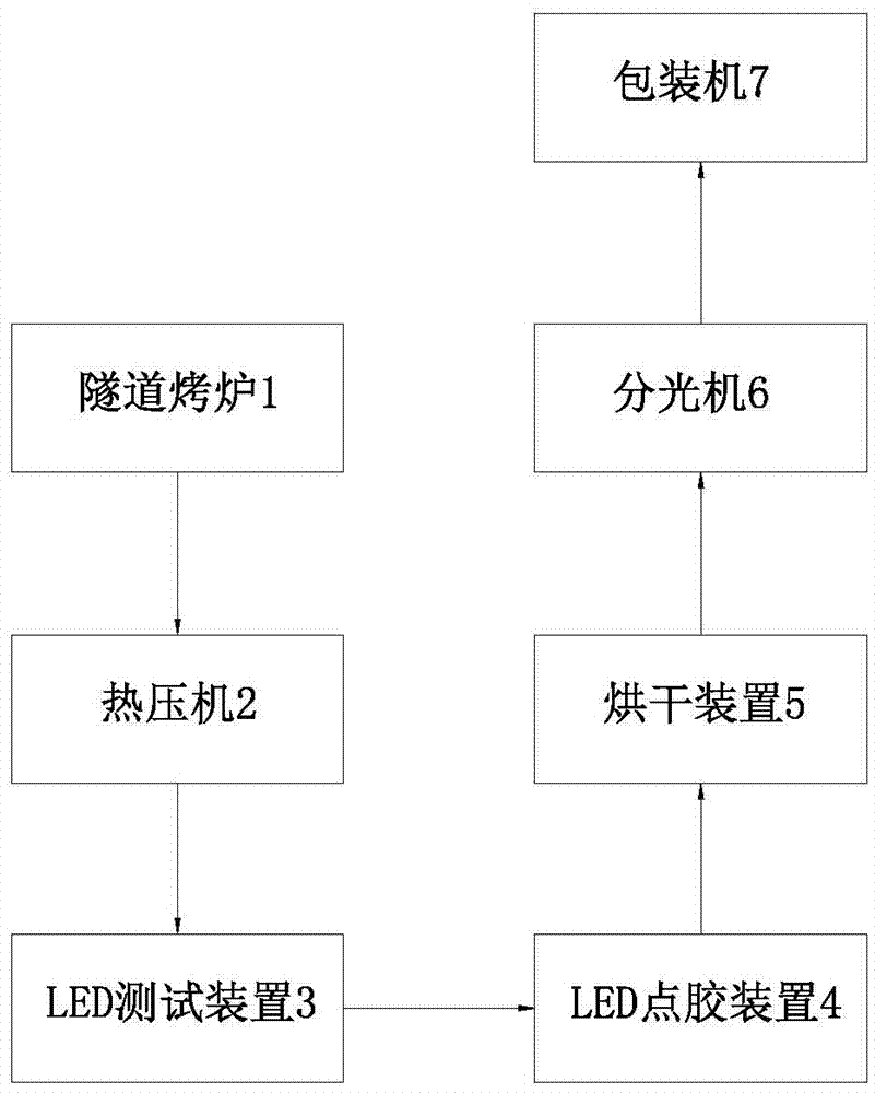
[0028] Such as figure 1 As shown, an LED crystal bonding equipment includes a tunnel oven 1, a hot press 2, an LED testing device 3, an LED dispensing device 4, a drying device 5, a spectroscope 6 and a packaging machine 7 in sequence according to the material conveying direction. Each equipment is docked through the conveyor track, which can realize automated production.

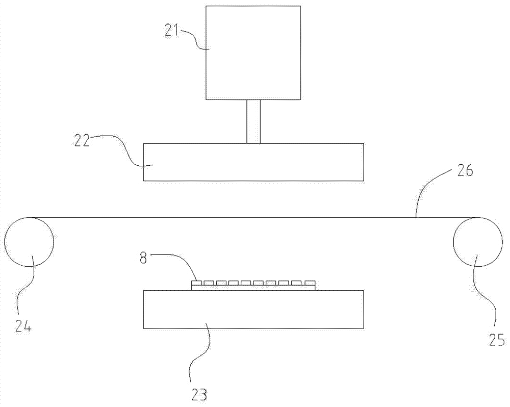
[0029] The principle of automated production: use conventional production equipment to realize glue dispensing and placement of flip-chip LED chips 8. After completing a unit of product, directly send it to tunnel oven 1, after 5 minutes of high temperature baking at 120 ℃, and then The product is sent to the hot press 2, the sensor detects the product and sends it to the hot pressing position of the hot press 2, and the hot press 2 heats the product; after completion, the product is...


PUM


Abstract

A die bonding method for flip LED chips comprises the following steps: (1) designing a flip circuit board, wherein the periphery of the flip circuit board except a die bonding area is coated with highly-reflective ink, the die bonding area has a positive pad and a negative pad, and a block clearance is formed between the positive pad and the negative pad; (2) dropping longitudinal conductive adhesive on the die bonding area to cover the positive pad and the negative pad, and placing a flip LED chip in the die bonding area; (3) placing the flip LED chip at 100-130 DEG C for 4-6 minutes to cure the longitudinal conductive adhesive; (4) hot pressing the flip LED chip in a hot press, wherein the pressure is 80-120kpa, the heating temperature is 130-170 DEG C, and the time lasts 50-70 seconds; and (5) completing die bonding of the flip LED chip. The phenomenon that the chip electrodes may be short-circuited in the traditional die bonding process is avoided.

Description

Technical field [0001] The invention relates to LED chip bonding, in particular to a flip chip LED chip bonding method. Background technique [0002] The LED chip is made of semiconductor materials, and the core of the chip is a PN junction. When a corresponding voltage is applied to both ends of the PN junction, it can emit light to the outside. With the continuous improvement of the power requirements of the LED light source, the area of ​​the LED chip is getting larger and larger, and the application of the flip chip (Flipchip) due to its advantages such as large effective light-emitting area is also becoming wider and wider. The bonding process of flip chip is different from that of formal chip. The electrode of the flip chip is set at the bottom of the LED chip. When bonding, the bonding glue or solder paste is applied on the pad, and then the flip chip is placed on the Cure on the pad. For example, a Chinese patent, a method of LED flip chip bonding with publication numbe...

Claims


Application Information

Patent Timeline
Patent Type & Authority Applications(China)
IPC IPC(8): H01L33/62H01L33/60
CPCH01L33/62H01L33/60H01L2933/0058H01L2933/0066
Inventor 陈焕杰吴江辉
Owner GUANGDONG RAYTON INTELLIGENT OPTO CO LTD
Why Eureka
Try Eureka