Supercharge Your Innovation With Domain-Expert AI Agents!

Light-emitting diode display substrate, manufacturing method thereof, and display device

A technology of light-emitting diodes and manufacturing methods, which is applied in the direction of diodes, semiconductor/solid-state device manufacturing, and electrical components, and can solve problems affecting product yield, rough metal boundaries, and dark spots, so as to ensure product yield and reduce composition process, to avoid the effect of short circuit

Active Publication Date: 2018-04-20
BOE TECH GRP CO LTD
View PDF6 Cites 0 Cited by
  • Summary
  • Abstract
  • Description
  • Claims
  • Application Information

AI Technical Summary

Problems solved by technology

If it is considered not to use the pixel definition layer, since the metal boundary of the reflective anode is relatively rough, and the layers in the OLED device are very thin, a short circuit may occur at the boundary of the anode during the evaporation process, eventually forming a dark spot, which affects the product yield.

Method used


Image

  • Light-emitting diode display substrate, manufacturing method thereof, and display device
  • Light-emitting diode display substrate, manufacturing method thereof, and display device
  • Light-emitting diode display substrate, manufacturing method thereof, and display device

Examples


Embodiment Construction

[0041] Specific embodiments of the present invention will be described in detail below in conjunction with the accompanying drawings. It should be understood that the specific embodiments described here are only used to illustrate and explain the present invention, and are not intended to limit the present invention.

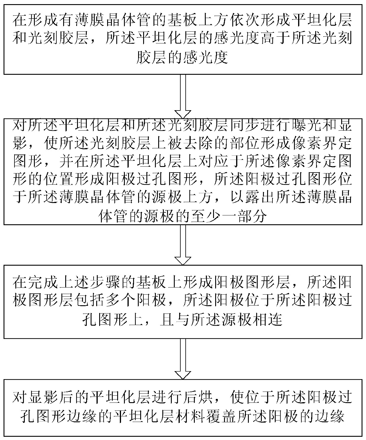
[0042] The invention provides a method for manufacturing a photodiode display substrate, such as figure 1 Shown, described preparation method comprises the following steps:

[0043] sequentially forming a planarization layer and a photoresist layer on the substrate on which the thin film transistor is formed, the sensitivity of the planarization layer is higher than that of the photoresist layer;

[0044] Carrying out gray-scale exposure and development on the planarization layer and the photoresist layer, so that the photoresist is completely removed and the part of the planarization layer is partially removed to form a pixel definition pattern, and in the pla...


PUM


Abstract

The invention discloses a light-emitting diode display substrate, a manufacturing method thereof, and a display device. The manufacturing method includes: sequentially forming a planarization layer and a photoresist layer on the substrate on which the thin film transistor is formed, the sensitivity of the planarization layer is higher than that of the photoresist layer; Exposure and development, so that the removed part of the photoresist layer forms a pixel defining pattern, and forms an anode via hole pattern on the planarization layer corresponding to the position of the pixel defining pattern, and the anode via hole pattern is located at the source of the thin film transistor Above; forming an anode pattern layer on the substrate that has completed the above steps, the anode pattern layer includes a plurality of anodes, and the anodes are located on the anode via pattern and connected to the source; post-baking the developed planarization layer, so that The planarization layer material located on the edge of the anode via pattern covers the edge of the anode. The invention can reduce process steps and reduce production cost.

Description

technical field [0001] The present invention relates to the field of display technology, in particular to a light-emitting diode display substrate, a manufacturing method thereof, and a display device including the light-emitting diode display substrate. Background technique [0002] In the field of display technology, photodiode display panels have become a hot spot in modern display research because of their advantages such as high response speed, high color gamut, high contrast, wide viewing angle, ultra-thin, and low power consumption. Light-emitting diode display panels include bottom emission and top emission modes. In the bottom emission mode, the white light OLED is manufactured under the TFT array, and the manufacturing process is relatively simple, but the metal wiring will block the light emitted by the OLED, resulting in a decrease in the aperture ratio, making it difficult to manufacture high PPI products. In the top emission mode, the white light OLED emits li...

Claims


Application Information

Patent Timeline
Patent Type & Authority Patents(China)
IPC IPC(8): H01L51/56H01L27/32H01L51/52H10K99/00
CPCH10K59/124H10K59/122H01L27/1248H01L27/1288H10K59/38H10K71/231H10K59/131H10K71/00H10K71/166H01L27/1214H01L29/78627
Inventor 方金钢宋泳锡孙宏达李伟
Owner BOE TECH GRP CO LTD
Features
  • R&D
  • Intellectual Property
  • Life Sciences
  • Materials
  • Tech Scout
  • Unparalleled Data Quality
  • Higher Quality Content
  • 60% Fewer Hallucinations
Learn More