ITO conductive film for touch sensor, preparation method of ITO conductive film and application of ITO conductive film to touch screen
A technology of touch sensor and conductive film, which is applied in the direction of cable/conductor manufacturing, conductive layer on insulating carrier, instrument, etc. It can solve the problems of abnormal response of sensors in the visible area, uneven etching of ITO layer, and residue of crystalline ITO, etc. Achieve the effect of avoiding short circuit between wires, uniform surface and good conductivity
- Summary
- Abstract
- Description
- Claims
- Application Information
AI Technical Summary
Problems solved by technology
Method used
Image

Examples
Embodiment 1
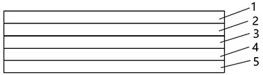
[0037] A kind of ITO conductive film for touch sensor, such as figure 1 As shown, it includes a substrate layer 5, and also includes an adhesive layer 4, a crystallization transition layer 3, an easy crystallization layer 2 and a metal conductive layer 1 sequentially deposited on the surface of the substrate layer 5; the crystallization transition layer 3 is in a crystalline state The first ITO layer, the easily crystallizable layer 2 is an amorphous second ITO layer.
[0038]Wherein, the material of the substrate layer 5 is PET with a thickness of 125 μm, and the bonding layer 4 is SiO with a thickness of 15 nm. 2 layer, the thickness of the first ITO layer is 5nm, the thickness of the second ITO layer is 20nm; the metal conductive layer 1 is a Cu layer with a thickness of 300nm.
[0039] The preparation method of the ITO conductive thin film for the touch sensor, the steps are to deposit the bonding layer 4, the first ITO layer 3, the second ITO2 layer and the metal conduct...
Embodiment 2
[0045] An ITO conductive film for a touch sensor, comprising a substrate layer, and further comprising an adhesive layer, a crystallization transition layer, an easy crystallization layer and a metal conductive layer deposited on the surface of the substrate layer in sequence; the crystallization transition layer is in a crystalline state The first ITO layer, the easy-to-crystallize layer is an amorphous second ITO layer.
[0046] Wherein, the material of the substrate layer is PET with a thickness of 125 μm, and the bonding layer is Si with a thickness of 15 nm. 3 N 4 layer, the thickness of the first ITO layer is 5 nm, the thickness of the second ITO layer is 20 nm; the metal conductive layer is an Ag layer with a thickness of 300 nm.
[0047] The preparation method of the ITO conductive film for the touch sensor comprises the steps of sequentially depositing a bonding layer, a first ITO layer, a second ITO layer and a metal conductive layer on the surface of the substrate ...
Embodiment 3
[0053] An ITO conductive film for a touch sensor, comprising a substrate layer, and further comprising an adhesive layer, a crystallization transition layer, an easy crystallization layer and a metal conductive layer deposited on the surface of the substrate layer in sequence; the crystallization transition layer is in a crystalline state The first ITO layer, the easy-to-crystallize layer is an amorphous second ITO layer.
[0054] Wherein, the material of the substrate layer is PMMA with a thickness of 125 μm, and the bonding layer is SiO with a thickness of 50 nm. 2 layer, the thickness of the first ITO layer is 10 nm, the thickness of the second ITO layer is 10 nm; the metal conductive layer is a Cu layer with a thickness of 300 nm.
[0055] The preparation method of the ITO conductive film for the touch sensor comprises the steps of sequentially depositing a bonding layer, a first ITO layer, a second ITO layer and a metal conductive layer on the surface of the substrate lay...
PUM
| Property | Measurement | Unit |
|---|---|---|
| thickness | aaaaa | aaaaa |
| thickness | aaaaa | aaaaa |
| thickness | aaaaa | aaaaa |
Abstract
Description
Claims
Application Information