Cu/ceramic material joint, method for manufacturing Cu/ceramic material joint, and substrate for power module

A manufacturing method and joint body technology, applied in the direction of ceramic layered products, chemical instruments and methods, applications, etc., can solve the problems of reduced joint rate, inability to provide reliable power module substrates, and degradation of ceramic substrates

Active Publication Date: 2016-03-30
MITSUBISHI MATERIALS CORP
View PDF7 Cites 16 Cited by
  • Summary
  • Abstract
  • Description
  • Claims
  • Application Information

AI Technical Summary

Problems solved by technology

Therefore, there is a problem that ceramic substrates may be deteriorated when joined by active metal brazing
Here, if the bonding temperature is lowered, the brazing filler metal cannot sufficiently react with the c

Method used


Image

  • Cu/ceramic material joint, method for manufacturing Cu/ceramic material joint, and substrate for power module
  • Cu/ceramic material joint, method for manufacturing Cu/ceramic material joint, and substrate for power module
  • Cu/ceramic material joint, method for manufacturing Cu/ceramic material joint, and substrate for power module

Examples


no. 1 approach

[0051] First, combine Figure 1 to Figure 5 A first embodiment of the present invention will be described.

[0052] The Cu-ceramic bonded body of the present embodiment includes a power module substrate 10 constituted by bonding a ceramic substrate 11 as a ceramic component and a copper plate 22 (circuit layer 12 ) as a copper component.

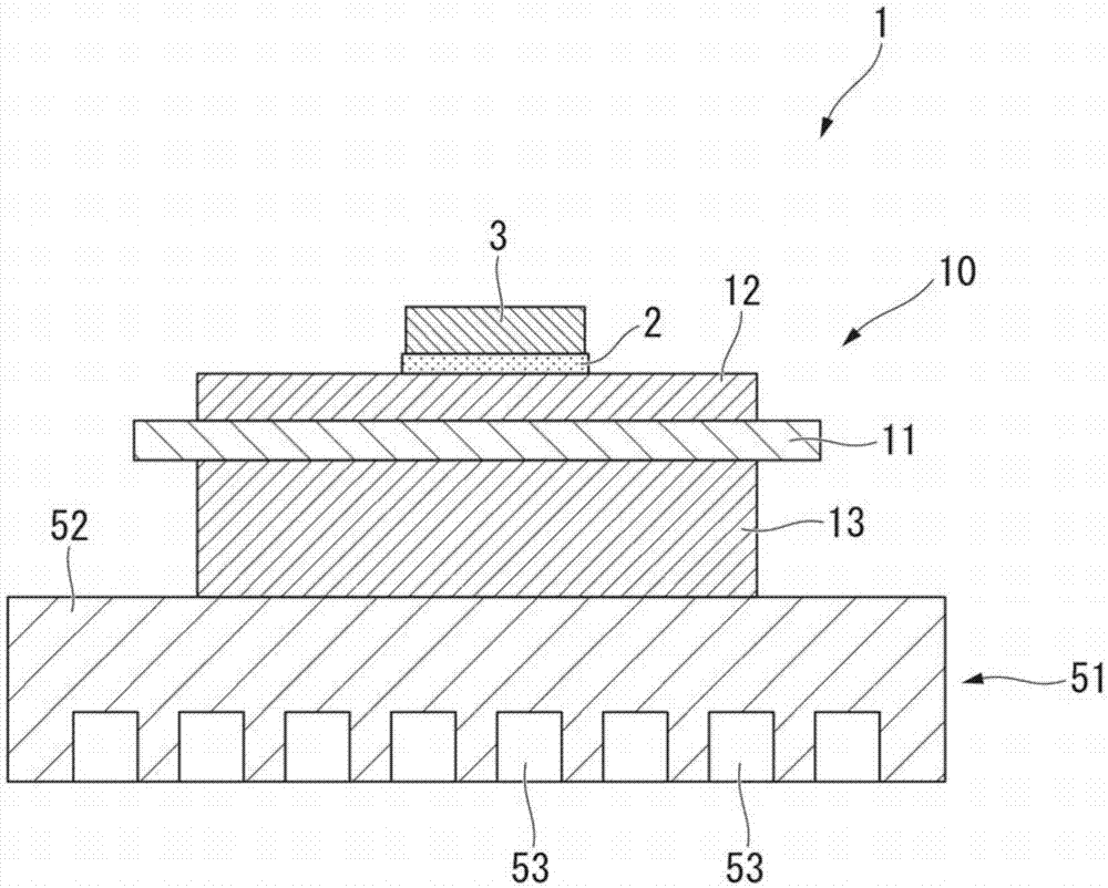
[0053] exist figure 1 The power module substrate 10 according to the first embodiment of the present invention and the power module 1 using the power module substrate 10 are shown in FIG.

[0054] The power module 1 includes: a power module substrate 10, on one side of the power module substrate 10 ( figure 1 The semiconductor element 3 bonded via the solder layer 2 is disposed on the other side of the power module substrate 10 ( figure 1 The lower side of the middle) radiator 51.

[0055] Among them, the solder layer 2 is, for example, a Sn-Ag-based, Sn-In-based, or Sn-Ag-Cu-based solder material.

[0056] The substrate 10 for a power ...

no. 2 approach

[0096] Second, combine Figure 6 to Figure 10 A second embodiment of the present invention will be described.

[0097] The Cu-ceramic bonded body of the present embodiment includes a power module substrate 110 constituted by joining a ceramic substrate 111 as a ceramic member and a copper plate 122 (circuit layer 112 ) and copper plate 123 (metal layer 113 ) as copper members.

[0098] Figure 6 2 shows a power module substrate 110 according to a second embodiment of the present invention and a power module 101 using the power module substrate 110 .

[0099] The power module 101 includes a power module substrate 110, and on one side of the power module substrate 110 ( Figure 6 The semiconductor element 103 bonded via the first solder layer 102 is disposed on the other side of the power module substrate 110 ( Figure 6 The lower side of the middle) radiator 151.

[0100] The power module substrate 110 includes a ceramic substrate 111, and is disposed on one surface of the ...

no. 3 approach

[0135] Second, combine Figure 11 to Figure 15 A third embodiment of the present invention will be described.

[0136] In the Cu-ceramic bonded body of the present embodiment, if Figure 11 As shown, a power module substrate 210 is provided, and the power module substrate 210 is constituted by bonding a ceramic substrate 211 as a ceramic component and a copper plate 222 (circuit layer 212 ) as a copper component.

[0137] The ceramic substrate 211 is made of high insulating Al 2 o 3 (alumina) configuration, and its structure is the same as that of the second embodiment.

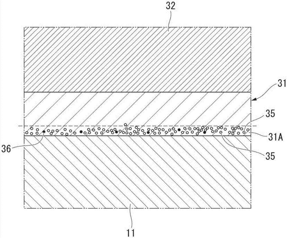
[0138] Such as Figure 14 As shown, the circuit layer 212 is formed by bonding a copper plate 222 made of copper or a copper alloy to one surface of the ceramic substrate 211, and its structure is the same as that of the second embodiment.

[0139] Among them, such as Figure 14 As shown, the ceramic substrate 211 and the circuit layer 212 (copper plate 222 ) are bonded using Ag—Ti based solder paste 224 ...


PUM

PropertyMeasurementUnit
Thicknessaaaaaaaaaa
Thicknessaaaaaaaaaa
Yield strengthaaaaaaaaaa

Abstract

A Cu/ceramic material joint according to the present invention is produced by joining a copper member comprising copper or a copper alloy to a ceramic member comprising AlN or Al2O3 using a joint material containing Ag and Ti, wherein a Ti compound layer comprising a Ti nitride or a Ti oxide is formed at the joint interface between the copper member and the ceramic member, and Ag particles are dispersed in the Ti compound layer.

Description

technical field [0001] The present invention relates to a method by combining copper parts made of copper or copper alloy with AlN or Al 2 o 3 A Cu-ceramic bonded body obtained by bonding the constituted ceramic components, a method for producing the Cu-ceramic bonded body, and a substrate for a power module composed of the Cu-ceramic bonded body. [0002] This application claims priority based on Patent Application No. 2013-204060 for which it applied in Japan on September 30, 2013, and uses the content here. Background technique [0003] A semiconductor device such as an LED or a power module has a structure in which a semiconductor element is bonded to a circuit layer made of a conductive material. [0004] Power semiconductor elements for high-power control used to control wind power generation, electric vehicles, hybrid vehicles, etc., generate a lot of heat. Therefore, as substrates for mounting such power semiconductor elements, for example, substrates made of AlN ...

Claims


Application Information

Patent Timeline
IPC IPC(8): C04B37/02B32B15/04B32B18/00H01L23/12H01L23/13H01L23/36H01L23/373H01L25/07H01L25/18
CPCH01L25/07H01L25/18C04B37/026C04B2235/6567C04B2237/125C04B2237/127C04B2237/343C04B2237/345C04B2237/36C04B2237/366C04B2237/407C04B2237/55C04B2237/60C04B2237/704C04B2237/706C04B2237/708C04B2237/72H01L2224/32225H01L2924/0002H01L23/3735H01L23/3736H01L23/4006H01L23/473H01L2023/4062B32B9/041B32B15/20B32B2457/18B32B2605/00B32B9/005C04B2235/6565C04B2237/12B32B7/12B32B2264/105B32B2457/14H01L2924/00
Inventor 寺崎伸幸长友义幸
Owner MITSUBISHI MATERIALS CORP
Why Eureka
Try Eureka