Method for automatic positioning of TSV (Through Silicon Vias) through utilizing smallest enclosing circle

An automatic positioning and enclosing circle technology, applied in special data processing applications, instruments, electrical digital data processing, etc., can solve the problems of increased wiring difficulty, increased interconnection length, and increased interconnection length, so as to shorten the interconnection length Effect

Inactive Publication Date: 2016-04-06
BEIJING UNIV OF TECH
View PDF3 Cites 3 Cited by
  • Summary
  • Abstract
  • Description
  • Claims
  • Application Information

AI Technical Summary

Problems solved by technology

Due to the increase in the number of transistors in the chip, the length of the interconnection increases, causing the power consumption of the interconnection to gradually exceed the power consumption of the transistor and become the main power consumption of the chip.
The increase in interconnect length also leads to increased routing difficulty and other issues
As the size of the transistor shrinks, the semiconductor manufacturing process is getting closer and closer to its physical limit, making it difficult to continue shrinking the size of the transistor

Method used


Image

  • Method for automatic positioning of TSV (Through Silicon Vias) through utilizing smallest enclosing circle
  • Method for automatic positioning of TSV (Through Silicon Vias) through utilizing smallest enclosing circle
  • Method for automatic positioning of TSV (Through Silicon Vias) through utilizing smallest enclosing circle

Examples


Embodiment Construction

[0028] The present invention will be further described below in conjunction with the accompanying drawings.

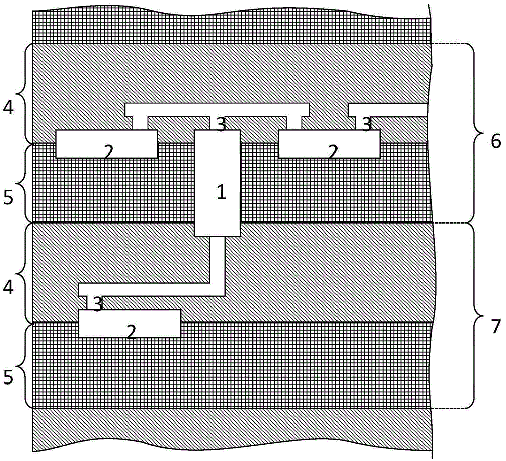
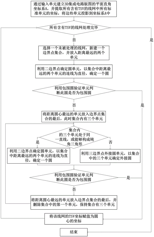
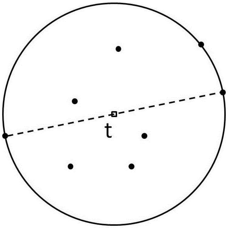
[0029] Such as figure 1 Shown is a schematic cross-sectional structure diagram of two layers of a 3D integrated circuit chip. The 3D integrated circuit chip includes a TSV1, a standard cell 2, a metal interconnection line 3, a metal layer 4, a substrate 5, an upper chip 6 and a lower chip 7; The invention includes four units, namely an input unit, a circle unit for determining two boundary points, a circumscribed circle unit for three boundary points, and an enclosing circle verification unit; the 3D integrated circuit in the present invention is a three-dimensional chip structure, and each of the 3D integrated circuits The layers are two-dimensional chips; the upper chip 6 and the lower chip 7 represent the general structure of the two layers in the 3D integrated circuit; Inter-communication; the standard unit 2 in the chip is the basic component of the integrated ci...


PUM


Abstract

The invention discloses a method for automatic positioning of TSVs (Through Silicon Vias) through utilizing a smallest enclosing circle, belonging to the field of circuit design. The method comprises the following steps of firstly, establishing a rectangular plane coordinate system for layout of a 3D integrated circuit and projecting coordinates of all standard units in all nets containing the TSVs into the coordinate system; secondly, respectively processing each net containing the TSV; thirdly, forming a discrete point set through all standard units in the nets and utilizing a smallest enclosing circle algorithm to solve the smallest enclosing circle of discrete points, wherein the center coordinates are coordinates of all TSVs of the nets; and lastly, processing the all nets to obtain the coordinates of all TSVs in the 3D integrated circuit. The method has the following beneficial effects that the positions of the TSVs of all nets can be determined; and the positions of the TSVs are determined by utilizing the smallest enclosing circle, so that the method is beneficial to shortening of an interconnection length of the 3D integrated circuit.

Description

technical field [0001] The invention relates to an automatic layout technology for a 3D integrated circuit, which belongs to the field of circuit design, and in particular to a TSV automatic positioning method for a 3D integrated circuit. Background technique [0002] With the development of the integrated circuit industry, the number of transistors in the integrated circuit chip is gradually increasing, and the size of the transistors is also getting smaller and smaller. Due to the increase in the number of transistors in the chip, the length of the interconnection increases, causing the power consumption of the interconnection to gradually exceed the power consumption of the transistors and become the main power consumption of the chip. The increase in interconnect length can also lead to increased routing difficulties, among other problems. As the size of the transistor shrinks, the semiconductor manufacturing process is getting closer and closer to its physical limit, m...

Claims


Application Information

Patent Timeline
Patent Type & Authority Applications(China)
IPC IPC(8): G06F17/50
CPCG06F30/39
Inventor 侯立刚赵未付婧妍杨扬彭晓宏耿淑琴汪金辉
Owner BEIJING UNIV OF TECH
Why Eureka
Try Eureka