Gate driving unit, gate driving circuit and display device
一种栅极驱动、驱动单元的技术,应用在栅极驱动电路及显示装置,栅极驱动单元领域,能够解决漏电、限制电路工作频率、增大栅极驱动电路的输出脉冲下降延迟等问题
- Summary
- Abstract
- Description
- Claims
- Application Information
AI Technical Summary
Problems solved by technology
Method used
Image
Examples
Embodiment 1
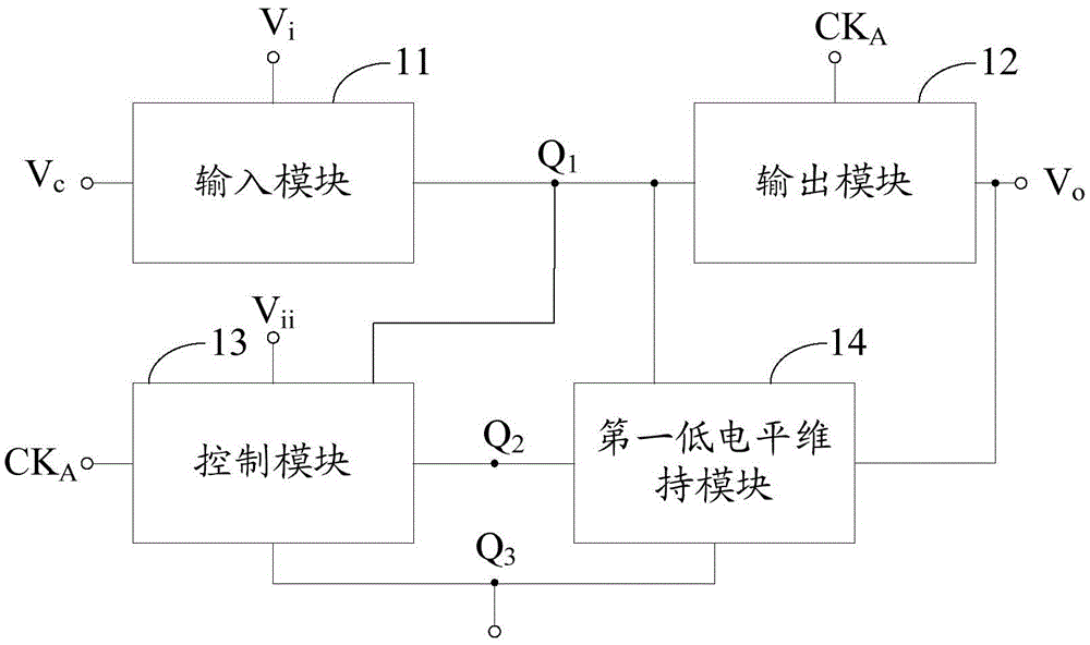
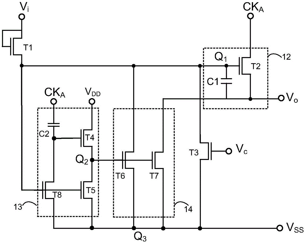
[0052] refer to figure 2 , in a specific implementation manner of the gate driving unit of the present invention, the input module 11 includes a first transistor T1 and a third transistor T3. Wherein, the gate of the first transistor T1 and the first pole are short-circuited as the pulse signal input terminal of the input module 11 for inputting the first pulse signal V i , the second pole of the first transistor T1 and the first pole of the third transistor T3 are connected to the first control node Q 1 , the second pole of the third transistor T3 is connected to the low-level node Q 3 , the gate of the third transistor T3 is used as the first pull-down control terminal of the input module 11 for inputting the first control signal V c .
[0053] The output module 12 includes a second transistor T2, and further includes a first capacitor C1. Wherein, the gate of the second transistor T2 serves as the drive control terminal of the output module 12 and is connected to the f...
Embodiment 2
[0068] refer to Figure 5 , Figure 5 It is a schematic diagram of a specific circuit structure of another embodiment of the gate driving unit of the present invention. and figure 2 The main difference between the illustrated embodiments is that in this embodiment, the control module 13 further includes a fifteenth transistor T15. Wherein, the gate of the fifteenth transistor T15 is connected to the gate of the first transistor T1, and the first pole of the fifteenth transistor T15 is connected to the second control node Q 2 , the second pole of the fifteenth transistor T15 is connected to the low-level node Q 3 .
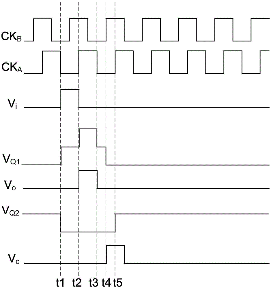
[0069] The gate of the fifteenth transistor T15 is controlled by the first pulse signal V i control. By adding the fifteenth transistor T15, at time t1, the first pulse signal V i The high-level control signal of the fifteenth transistor T15 is turned on, so that the second control node Q 2 Potential V Q2 quickly pulled low to V L , further suppressing t...
Embodiment 3
[0072] refer to Figure 6 , Figure 6 It is a schematic diagram of a specific circuit structure of another embodiment of the gate driving unit of the present invention. In this embodiment, with figure 2 The main difference of the illustrated embodiment is that the control module 13 further includes a ninth transistor T9 and a tenth transistor T10. The gate driving unit further includes a second low-level sustaining module 15, wherein the second low-level sustaining module 15 includes an eleventh transistor T11 and a twelfth transistor T12.
[0073] Wherein, the gate of the ninth transistor T9 is connected to the gate of the fourth transistor T4, the first pole of the ninth transistor T9 is used to input the third clock signal EXCK, the second pole of the ninth transistor T9 is connected to the gate of the tenth transistor T10 The first electrode, the gate of the eleventh transistor T11 and the gate of the twelfth transistor T12 are all connected to the fourth control node ...
PUM
 Abstract
Description
Claims
Application Information


