TFT array substrate and manufacturing method thereof

A technology of an array substrate and a manufacturing method, which is applied in the field of TFT array substrate and its manufacture, can solve the problems of large aperture ratio and insufficient aperture ratio of TFT array substrate, and achieve the effects of increasing aperture ratio, improving display quality and improving capacity

Active Publication Date: 2016-04-06
SHENZHEN CHINA STAR OPTOELECTRONICS TECH CO LTD
View PDF3 Cites 26 Cited by
  • Summary
  • Abstract
  • Description
  • Claims
  • Application Information

AI Technical Summary

Problems solved by technology

Compared with the above two existing designs of the charge sharing capacitor C, under the premise that the capacity of the charge sharing capacitor C is equal, the second design has a relatively small aperture ratio due to the small distance between the common electrode line M1 and the metal electrode M2. Larger, but even with the second design, the aperture ratio of the TFT array substrate is still insufficient

Method used


Image

  • TFT array substrate and manufacturing method thereof
  • TFT array substrate and manufacturing method thereof
  • TFT array substrate and manufacturing method thereof

Examples


Embodiment Construction

[0048] In order to further illustrate the technical means adopted by the present invention and its effects, the following describes in detail in conjunction with preferred embodiments of the present invention and accompanying drawings.

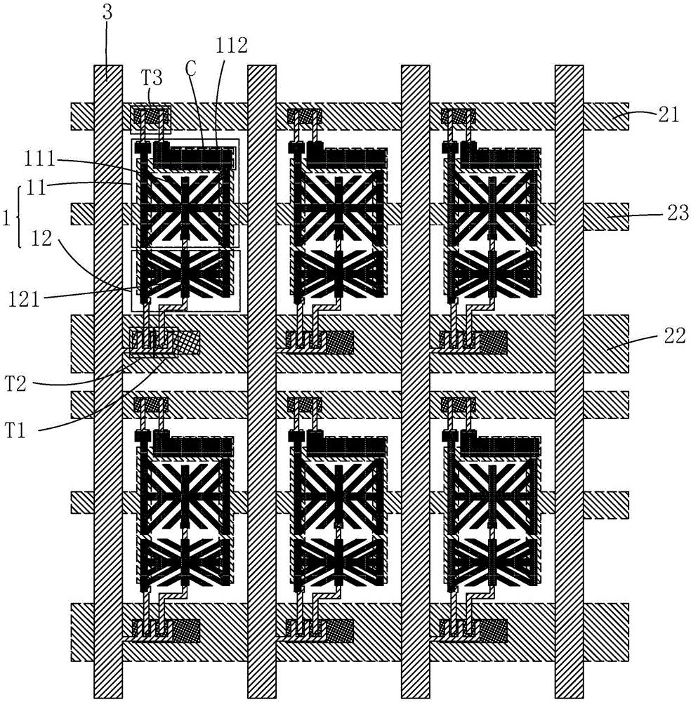
[0049] see Figure 4 and Figure 5 , The present invention firstly provides a TFT array substrate, including: a base substrate 10 , and several sub-pixel units P arrayed on the base substrate 10 .

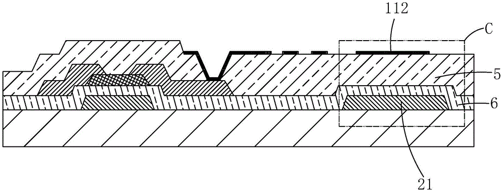
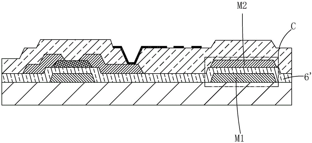
[0050] Each sub-pixel unit P includes: a first metal layer M10 patterned on the base substrate 10, a gate insulating layer 20 covering the first metal layer M10, and a gate insulating layer 20 disposed on the gate insulating layer. The semiconductor layer 30 on 20, the second metal layer M20 patterned on the semiconductor layer 30 and the gate insulating layer 20, the insulating protection layer 40 covering the second metal layer M20 and the gate insulating layer 20, And the patterned pixel electrode layer 50 disposed on the insulating protection...


PUM


Abstract

The invention provides a TFT array substrate and a manufacturing method thereof. The TFT array substrate is provided with a transparent conducting thin film electrode plate (503), a second metal electrode plate (202) and a common electrode wire (102), wherein the transparent conducting thin film electrode plate (503), a primary area pixel electrode (501) and a secondary area pixel electrode (502) are positioned on the same layer; the second metal electrode plate (202) is positioned on a second metal layer (M20); the common electrode wire (102) is positioned on a first metal layer (M10); a part of the common electrode wire (102), a part of the second metal electrode plate (202) and a part of the transparent conducting thin film electrode plate (503) are overlapped spatially, and the transparent conducting thin film electrode plate (503) is in contact with a part of the common electrode wire (102) through a second via hole (422) penetrating through an insulation protective layer (40) and a gate insulation layer (20); and a part of the common electrode wire (102), a part of the second metal electrode plate (202) and a part of the transparent conducting thin film electrode plate (503) form a charge sharing capacitor (C10) together, so that the capacity of the charge sharing capacitor can be improved, the aperture opening ratio is increased, and the display quality of a liquid crystal display panel is improved.

Description

technical field [0001] The invention relates to the field of display technology, in particular to a TFT array substrate and a manufacturing method thereof. Background technique [0002] Active thin film transistor liquid crystal display (ThinFilmTransistor-LCD, TFT-LCD) has been developed rapidly and widely used in recent years. Most of the liquid crystal displays currently on the market are backlight liquid crystal display devices, which include a liquid crystal display panel and a backlight module. Usually, the liquid crystal display panel is composed of a color filter substrate (ColorFilter, CF), a thin film transistor array substrate (ThinFilmTransistorArraySubstrate, TFTArraySubstrate), a liquid crystal (LiquidCrystal, LC) sandwiched between the color filter substrate and the TFT array substrate, and a sealant (Sealant). , its working principle is to control the rotation of the liquid crystal molecules in the liquid crystal layer by applying a driving voltage on the tw...

Claims


Application Information

Patent Timeline
Patent Type & Authority Applications(China)
IPC IPC(8): H01L27/12H01L21/77G02F1/1343G02F1/1362
CPCG02F1/134309G02F1/136213G02F2201/121G02F2201/123H01L27/1214H01L27/1255H01L27/1259
Inventor 徐向阳
Owner SHENZHEN CHINA STAR OPTOELECTRONICS TECH CO LTD
Why Eureka
Try Eureka