

Method and device for polishing semiconductor wafer
A grinding method and semiconductor technology, applied in grinding equipment, semiconductor devices, semiconductor/solid-state device manufacturing, etc., can solve the problems of measurement disturbance, lower measurement accuracy, longer feedback time, etc., and achieve the effect of shortening the moving time
- Summary
- Abstract
- Description
- Claims
- Application Information
AI Technical Summary
Problems solved by technology
Method used
Image

Examples
no. 1 Embodiment approach
[0037] First, a first embodiment of the present invention will be described with reference to the drawings.
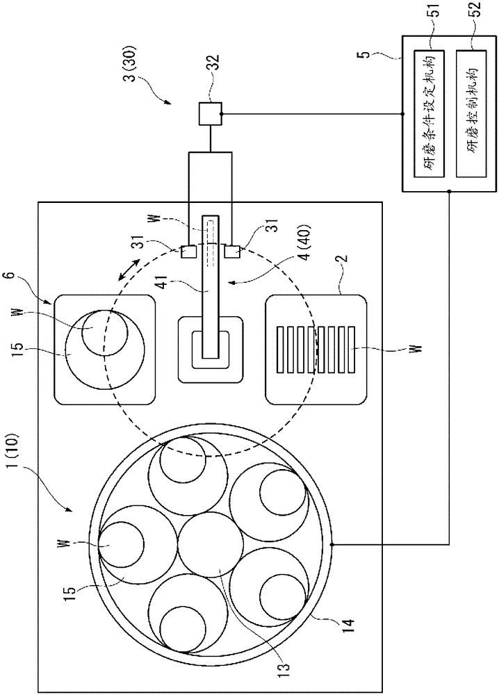
[0038] figure 1 It is a schematic diagram which shows the polishing apparatus of the semiconductor wafer of this invention.
[0039] like figure 1 As shown, the semiconductor wafer polishing apparatus of the present invention includes a polishing mechanism 1 , a storage tank 2 , a measuring mechanism 3 , a moving mechanism 4 , and a polishing condition setting mechanism 51 . Furthermore, the semiconductor wafer polishing apparatus of the present invention includes a storage unit 6 capable of storing a plurality of semiconductor wafers W and carriers 15 before polishing. In addition, in figure 1In the figure, the number of semiconductor wafers W stored in the carrier 15 is shown as one for simplicity of illustration, but in the present invention, it is not limited to one, and of course a plurality of semiconductor wafers can be stored.
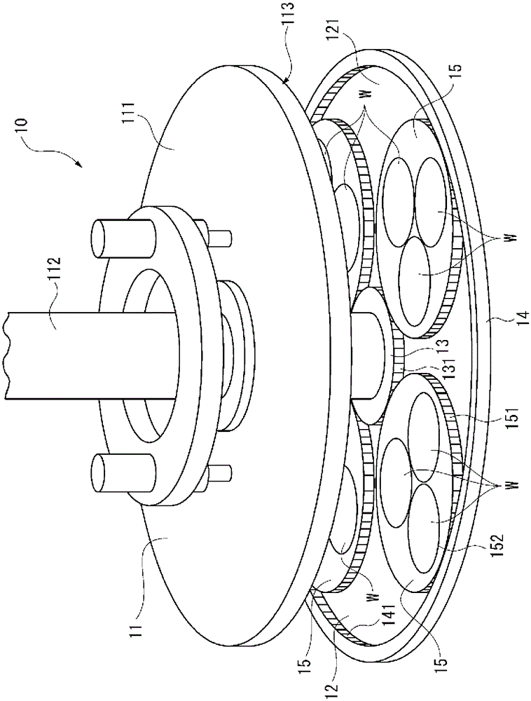
[0040] The grinding mechanis...
no. 2 Embodiment approach
[0121] Next, a second embodiment of the present invention will be described. In addition, since the structure of the semiconductor polishing apparatus of 2nd Embodiment is the same as that of 1st Embodiment mentioned above, description is abbreviate|omitted, and the polishing method of a semiconductor wafer is demonstrated.
[0122] 〈Pre-measurement process〉
[0123] First, the unpolished semiconductor wafer W stored in the storage unit 6 is transported to the measurement mechanism 3 by the moving mechanism 4, and the thickness of the unpolished bulk wafer W is measured in advance. The pre-measurement herein does not need to measure the entire surface of the semiconductor wafer W as in the measurement process performed after the grinding process, and only a desired portion of the semiconductor wafer W is measured by the measuring device unit 31 .
[0124] After the unpolished semiconductor wafer W is measured, the unpolished semiconductor wafer W is transported to the double-...
Embodiment 1
[0161] with the help of figure 1 The illustrated semiconductor wafer polishing apparatus performs double-sided polishing of a semiconductor wafer W having a diameter of 300 mm. In addition, the aqueous solution stored in the storage tank 2 is a citric acid aqueous solution with a concentration of 0.1% by mass maintained at 25°C.
[0162] First, the unpolished semiconductor wafer W and the carrier 15 are transported from the storage unit 6 to the double-side polishing apparatus 10 by the transport unit 40 . Then, a polishing liquid is supplied, and the semiconductor wafer W is polished on both sides under predetermined polishing conditions. After the double-side grinding, pure water is supplied to rinse the polished semiconductor wafer W.
[0163] After rinsing, the polished semiconductor wafer W is transferred from the double-side polishing apparatus 10 to the storage tank 2 by the transfer unit 40 . The semiconductor wafer W to be transported was immersed in the aqueous ci...
PUM
 Abstract
Description
Claims
Application Information