Wafer processing method

A processing method and wafer technology, applied in metal processing equipment, manufacturing tools, laser welding equipment, etc., can solve the problems that laser beams cannot be formed, wafers cannot be divided into pieces, etc., and achieve the effect of solving damage and less scattering

Active Publication Date: 2019-04-12
DISCO CORP
View PDF7 Cites 0 Cited by
  • Summary
  • Abstract
  • Description
  • Claims
  • Application Information

AI Technical Summary

Problems solved by technology

[0008] However, since the Nd:YAG pulsed laser has a wavelength of 1064nm close to the optical absorption end of silicon, a part of the laser beam is absorbed in the region sandwiching the focus point, so that a sufficient modified layer cannot be formed, and the wafer cannot be divided into The situation of each device chip

Method used


Image

  • Wafer processing method
  • Wafer processing method
  • Wafer processing method

Examples


Embodiment Construction

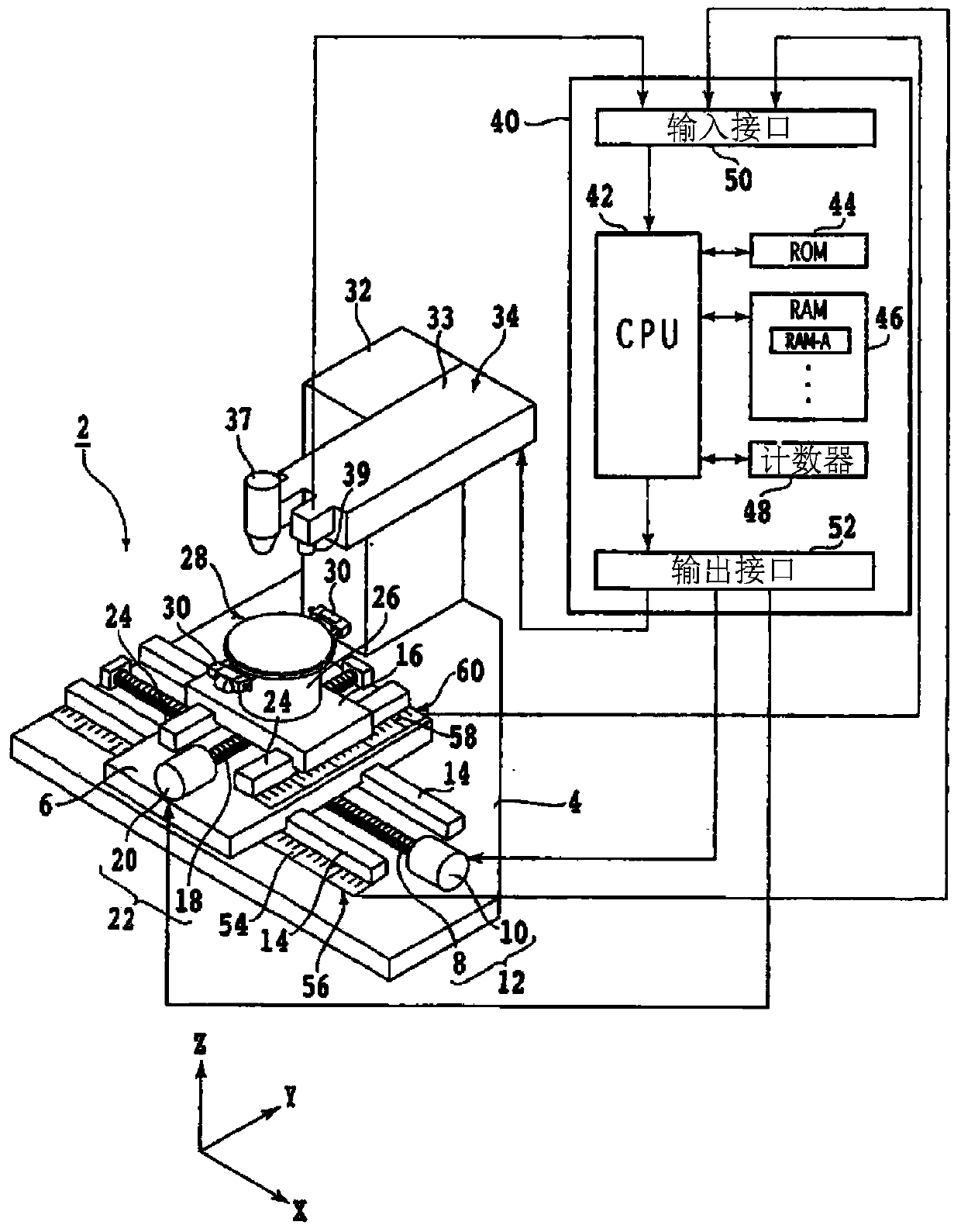
[0030] Hereinafter, embodiments of the present invention will be described in detail with reference to the drawings. when referring to figure 1 , a schematic perspective view of a laser processing apparatus 2 suitable for implementing the wafer processing method of the present invention is shown.

[0031] The laser processing device 2 includes a first slider 6 mounted on a stationary base 4 so as to be movable in the X-axis direction. The first slider 6 moves along a pair of guide rails 14 in the machining feed direction, that is, the X-axis direction, via a machining feed mechanism 12 composed of a ball screw 8 and a pulse motor 10 .

[0032] The second slider 16 is mounted on the first slider 6 so as to be movable in the Y-axis direction. That is, the second slider 16 moves along the pair of guide rails 24 in the index feeding direction, that is, the Y-axis direction, via the index feeding mechanism 22 constituted by the ball screw 18 and the pulse motor 20 .

[0033] On ...


PUM

PropertyMeasurementUnit
wavelengthaaaaaaaaaa
thicknessaaaaaaaaaa

Abstract

Provided is a method for processing a wafer, which processes a wafer made of silicon on which a plurality of devices are formed by dividing the front surface by a plurality of dividing lines, and includes: The converging point of the pulsed laser beam is positioned inside the wafer, and the area corresponding to the planned division line is irradiated with the pulsed laser beam from the back surface of the wafer, and the holding mechanism is processed and fed to the laser beam irradiation mechanism, and the inside of the wafer Forming a modified layer; a dividing step, after the modified layer forming step, applying an external force to the wafer and using the modified layer as the starting point of division to divide the wafer along the planned division line, in the modified layer forming step, after irradiation The portion from the center of the pulsed laser beam to the wafer to the outer periphery on the downstream side in the processing feed direction misses a part of the pulsed laser beam, and positions the converging point of the pulsed laser beam inside the wafer.

Description

technical field [0001] The present invention relates to a method of processing a wafer. After a modified layer is formed inside the wafer by irradiating a pulsed laser beam of a wavelength that is transparent to the wafer, an external force is applied to the wafer to divide the wafer into a plurality of wafers starting from the modified layer. device chip. Background technique [0002] Multiple devices such as IC and LSI are formed on the front side of a silicon wafer (hereinafter, sometimes simply referred to as a wafer) by dividing predetermined lines, and the silicon wafer is divided into individual device chips by a processing device, and the divided device chips are widely used. Used in various electronic devices such as mobile phones and personal computers. [0003] For dividing wafers, a dicing method using a cutting device called a dicing saw is widely used. In the dicing method, a cutting tool made of metal or resin with abrasive grains such as diamond solidified ...

Claims


Application Information

Patent Timeline
Patent Type & Authority Patents(China)
IPC IPC(8): B23K26/53B23K26/0622H01L21/78H01L21/268
CPCH01L21/268H01L21/78
Inventor 寺西俊辅
Owner DISCO CORP
Why Eureka
Try Eureka