A pulse width signal amplifying circuit

A pulse width signal and amplifying circuit technology, applied in the direction of electric pulse generator circuit, electrical components, electronic switches, etc., can solve the problems of IGBT tube damage, complicated circuit structure, increasing the difficulty of design, processing and debugging, etc., and reach the frequency band The effect of widening and simplifying the power supply

Inactive Publication Date: 2014-06-18
中国兵器工业第二〇二研究所
View PDF1 Cites 3 Cited by
  • Summary
  • Abstract
  • Description
  • Claims
  • Application Information

AI Technical Summary

Problems solved by technology

The circuit structure disclosed in this patent solves the driving problem of high-power insulated gate bipolar transistors (IGBT), but the circuit structure is complex, which increases the difficulty of design, processing and debugging. In addit

Method used


Image

  • A pulse width signal amplifying circuit
  • A pulse width signal amplifying circuit
  • A pulse width signal amplifying circuit

Examples


Embodiment 1

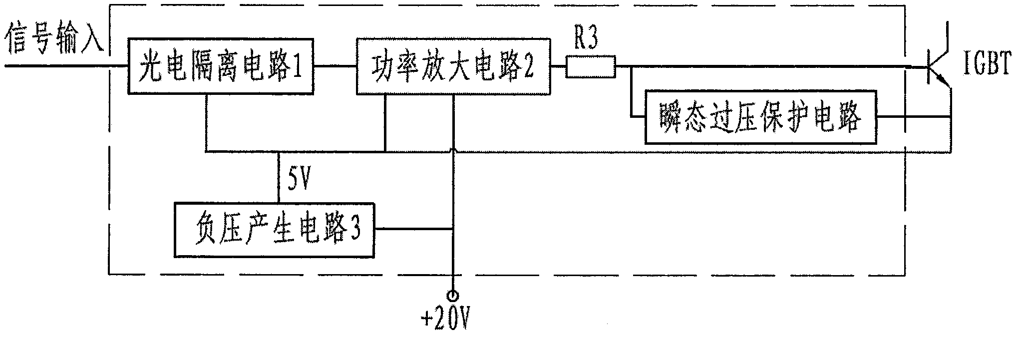
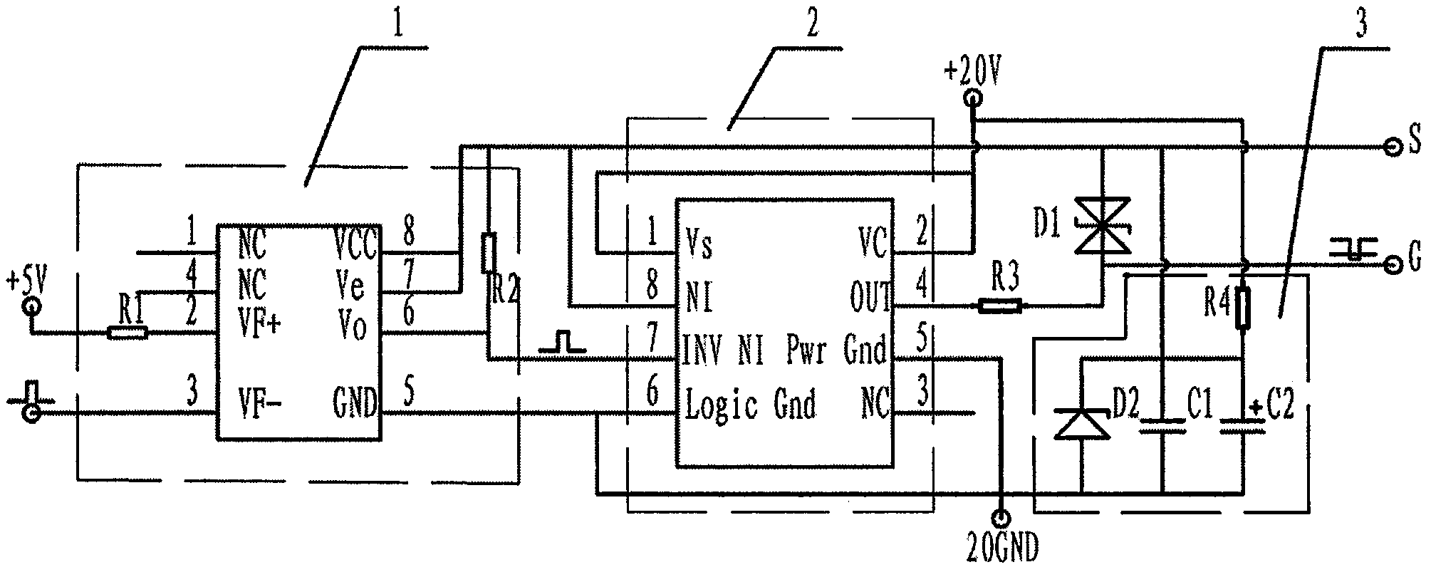
[0020] according to figure 2 The schematic diagram of the circuit is shown, and the implementation of the circuit is as follows: 1) Optocoupler isolation circuit, the optocoupler needs to use a high-speed, high-isolation voltage opto-isolation device to ensure the stability and reliability of high-frequency pulse width signal transmission. In this embodiment The ultra-high-speed isolation device 6N137 with an isolation voltage of 2500V is used. It is composed of an 850nm wavelength AlGaAs LED and an integrated detector. The transmission speed is 10MB / s, which meets the requirements of pulse width signal transmission. Resistors R1 and R2 are respectively selected as 1KΩ / 0.25W, 10KΩ / 0.25W can meet the requirements. After the optocoupler isolation, the delay of the rising edge of the signal is 12ns, and the delay of the falling edge is 50ns. The delay caused by the optocoupler isolation in one pulse width period is 62ns in total, which provides a guarantee for the high frequenc...


PUM

PropertyMeasurementUnit
Poweraaaaaaaaaa

Abstract

The invention discloses a pulse width signal amplification circuit. After the input pulse width signal is isolated by a photoelectric isolation circuit, it enters a power amplification circuit to amplify voltage and current, and the pulse width signal after voltage and current amplification is output to a power tube through a current limiting resistor. The gate of the power tube is used to complete the driving of the power tube; the transient overvoltage protection circuit is connected between the grid and the source of the power tube to suppress the voltage spike interference signal between the grid and the source; the negative voltage generating circuit generates 5V, Provided to the photoelectric isolation circuit and power amplifier circuit. The circuit structure of the present invention is simple and reliable, simplifies the power supply, eliminates the peak pulse voltage appearing at both ends of the gate and source of the power tube, widens the frequency band of the pulse width signal adapted to the drive circuit, and not only can be applied to insulated gate bipolar transistors, And it can be applied to metal oxide field effect transistors with higher frequency.

Description

technical field [0001] The invention relates to a driving technology of a power element, and mainly relates to technologies such as photoelectric isolation and power amplification of a switch control signal of a power electronic device. Background technique [0002] The emergence and application of various full-control power electronic devices such as GTO, MOSFET and IGBT have greatly promoted the development of power electronics technology. A drive circuit for a large-capacity insulated gate bipolar transistor is provided, including a photoelectric isolation stage (10), a power amplifier stage (20), a power supply (V2, V3), a shaping circuit (1), a shaping circuit (2), an electrical Level conversion circuit (30), the pulse width signal is output after passing through the photoelectric isolation stage 10, and the output signal is divided into two routes. The signal drives the MOS transistor T5 after passing through the level conversion circuit, and the MOS transistors T4 an...

Claims


Application Information

Patent Timeline
IPC IPC(8): H03K17/08H03K3/021H03K17/567
Inventor 位红军韩崇伟韩锋马捷李伟佟庆雨王国珍
Owner 中国兵器工业第二〇二研究所
Why Eureka
Try Eureka