Array substrate, preparing method of array substrate and display device

A technology for array substrates and display areas, applied in optics, instruments, electrical components, etc., can solve problems such as electrostatic breakdown of electronic components, open circuit or short circuit of data leads, and component damage

Active Publication Date: 2016-05-04
BOE TECH GRP CO LTD +1
View PDF12 Cites 10 Cited by
  • Summary
  • Abstract
  • Description
  • Claims
  • Application Information

AI Technical Summary

Problems solved by technology

The phenomenon of electrostatic discharge will lead to electrostatic breakdown of electronic components, which will cause open circuit or short circuit of data leads with thinner line width, resulting in damage to components, thereby reducing product quality

Method used


Image

  • Array substrate, preparing method of array substrate and display device
  • Array substrate, preparing method of array substrate and display device
  • Array substrate, preparing method of array substrate and display device

Examples


Embodiment Construction

[0034] The following will clearly and completely describe the technical solutions in the embodiments of the present invention with reference to the accompanying drawings in the embodiments of the present invention. Obviously, the described embodiments are only some, not all, embodiments of the present invention. Based on the embodiments of the present invention, all other embodiments obtained by persons of ordinary skill in the art without making creative efforts belong to the protection scope of the present invention.

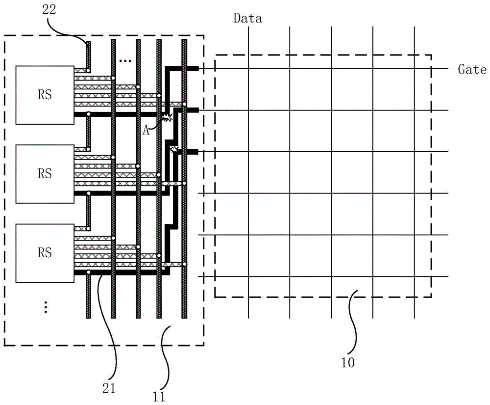
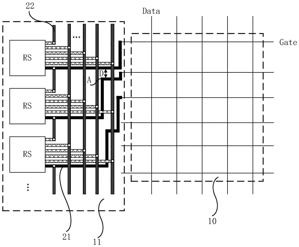
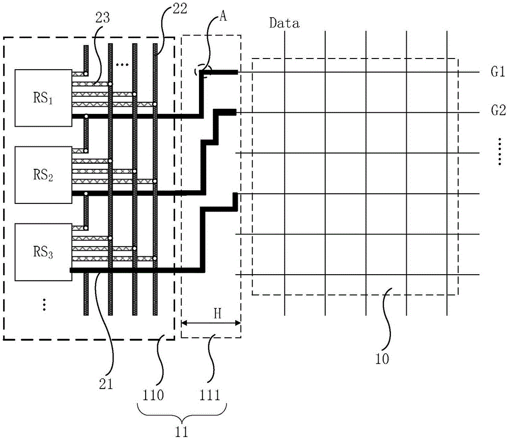
[0035] An embodiment of the present invention provides an array substrate, such as Figure 2a As shown, a display area 10 and a peripheral area 11 are included. Wherein, the display area 10 is provided with gate lines Gate and data lines Data which intersect horizontally and vertically. And the peripheral area 11 is provided with a first data lead 21 and at least two cascaded shift register units RS.

[0036] In addition, the peripheral area 11 may further i...


PUM


Abstract

The embodiment of the invention provides an array substrate, a preparing method of the array substrate and a display device and relates to the technical field of display. The wiring density of data leads in a densely-wired area can be reduced, and the probability of electrostatic discharge at a corner tip can be reduced. The array substrate comprises a display area and a peripheral area, wherein first data leads and at least two cascaded shifting register units are arranged in the peripheral area. The shifting register units are connected with grid lines in the display area through the first data leads. The minimum distance between every two adjacent first data leads is larger than or equal to a distance threshold value.

Description

technical field [0001] The present invention relates to the field of display technology, in particular to an array substrate, a preparation method thereof, and a display device. Background technique [0002] Thin Film Transistor-Liquid Crystal Display (ThinFilmTransistor-LiquidCrystalDisplay, TFT-LCD) array substrate such as figure 1 Shown includes a display area 10 and a peripheral area 11 for arranging drive components. Wherein, the display area 10 is provided with gate lines Gate and data lines Data which intersect horizontally and vertically. The peripheral area 11 is provided with a GOA (GateDriveronArray, array substrate row driver) circuit composed of a plurality of cascaded shift register units RS for progressively scanning the gate line Gate. [0003] Many data wires are provided in the existing peripheral area 11 , specifically, the shift register unit RS of each stage can be connected to the gate line Gate through the first data wire 21 . In addition, in order ...

Claims


Application Information

Patent Timeline
Patent Type & Authority Applications(China)
IPC IPC(8): G02F1/1362H01L27/12
CPCG02F1/136204G02F1/136286H01L27/124
Inventor 肖志莲裴晓光赵海生彭志龙温召虎
Owner BOE TECH GRP CO LTD
Why Eureka
Try Eureka