Method for manufacturing a thin film transistor array panel

Inactive Publication Date: 2011-07-21
SAMSUNG DISPLAY CO LTD
View PDF6 Cites 17 Cited by
  • Summary
  • Abstract
  • Description
  • Claims
  • Application Information

AI Technical Summary

Benefits of technology

[0031]According to the present invention, the photomask for the exposure of the Nega-PR organic layer has mosaic patterns formed in a direction (a first direction and a second direction) perpendicular and parallel to the wire therein in the areas corresponding to the pad area of the panel, wherein the mosaic patterns are formed with a metal pattern such as Cr having a line width of less than the resolution of a light exposer such that patterning light is transmitted thr

Problems solved by technology

If the signal lines are disposed too close to the pixel electrodes, excessive crosstalk may be generated, and this crosstalk may be due to the silicon nitride between the signal lines and the pixel electrodes being too thin and thus tending to function as a signal c

Method used


Image

  • Method for manufacturing a thin film transistor array panel
  • Method for manufacturing a thin film transistor array panel
  • Method for manufacturing a thin film transistor array panel

Examples


Embodiment Construction

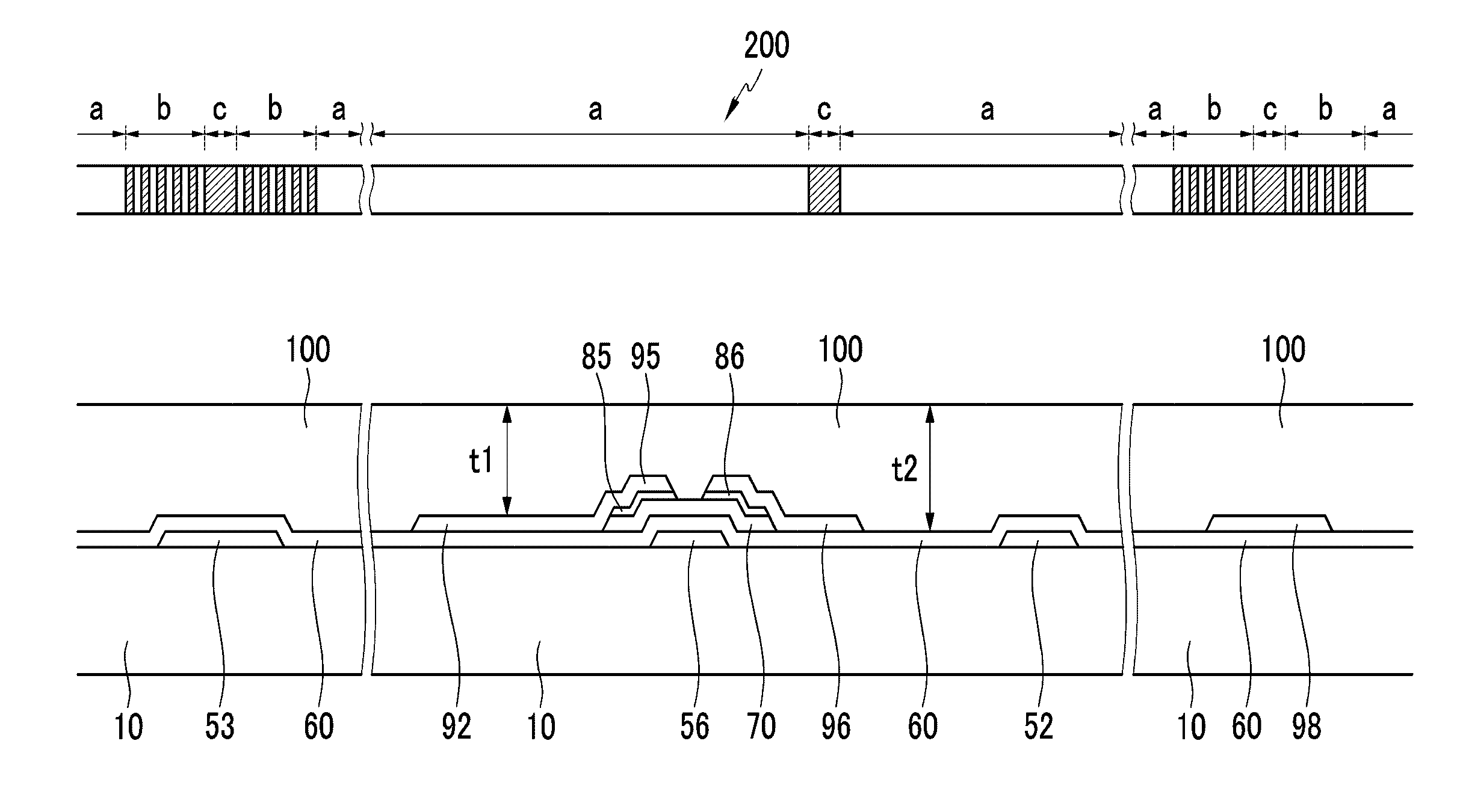
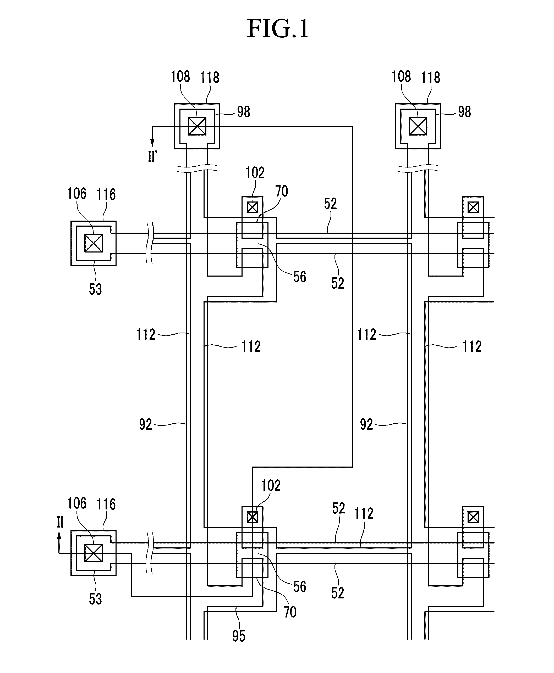
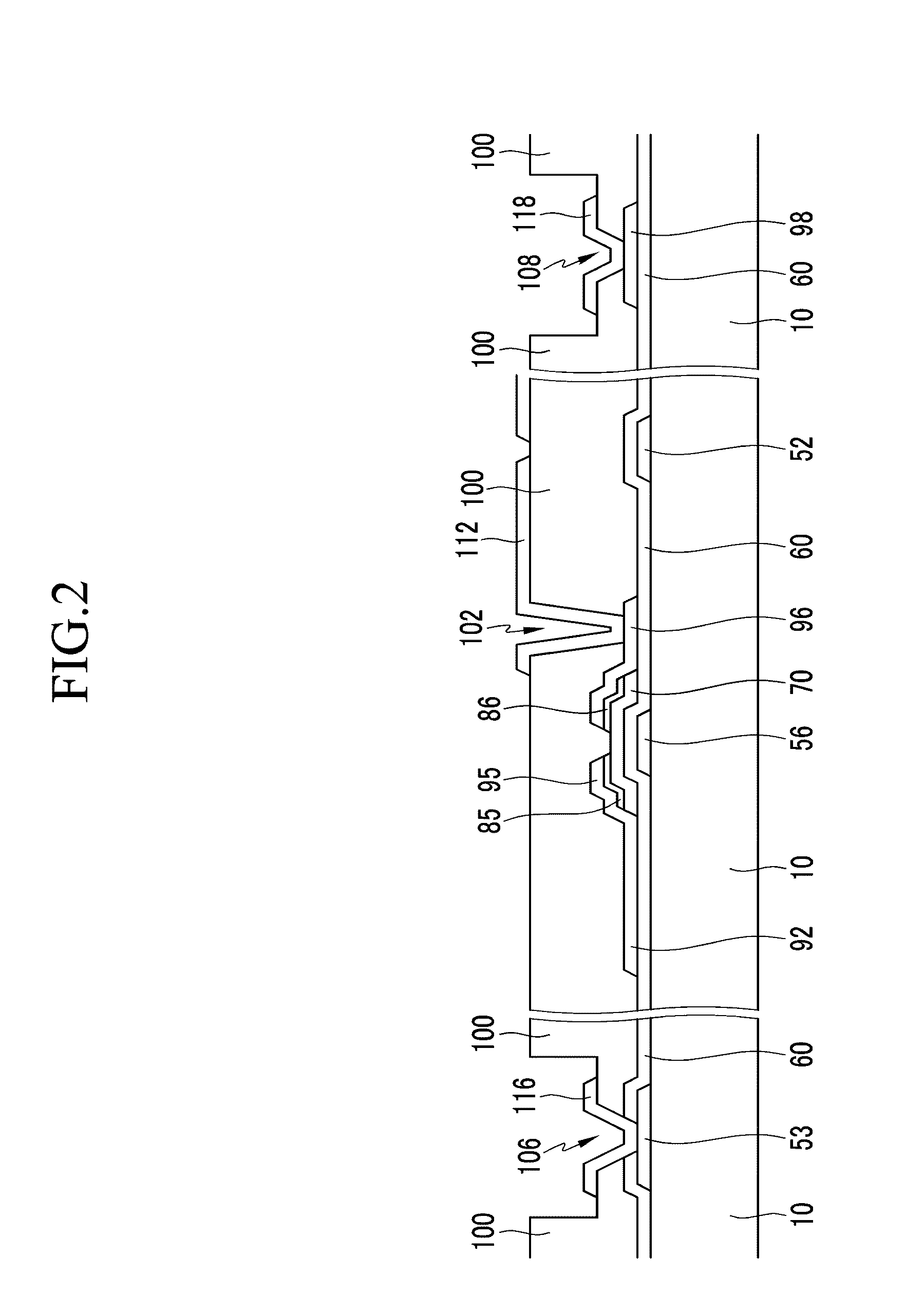
[0040]In the following detailed description, only certain exemplary embodiments of in accordance with the present disclosure have been shown and described, simply by way of illustration. As those skilled in the art would realize, the described embodiments may be modified in various different ways, all without departing from the spirit or scope of the present disclosure. Accordingly, the drawings and description are to be regarded as illustrative in nature and not restrictive, and like reference numerals designate like elements throughout the specification. Detailed descriptions of well-known techniques are omitted.

[0041]In the drawings, the thickness of layers, films, panels, regions, etc., are exaggerated for clarity. It will be understood that when an element such as a layer, film, region, or substrate is referred to as being “on” another element, it can be directly on the other element or intervening elements may also be present. On the other hand, when an element is referred to ...


PUM


Abstract

A thin film transistor display panel includes gate wiring formed on an insulation substrate and including gate lines, and gate electrodes and gate pads connected to the gate lines; a gate insulation layer covering the gate wiring; a semiconductor pattern formed over the gate insulation layer; data wiring formed over the gate insulation layer or the semiconductor pattern and including source electrodes, drain electrodes, and data pads; a protection layer including a Nega-PR type of organic insulating layer formed all over the semiconductor pattern and the data wiring, wherein the thickness of the Nega-PR type of organic insulating layer in both the gate and data pad regions is smaller than in the other regions; and a pixel electrode connected to the drain electrode. When exposing the Nega-PR type of passivation layer in the pad region during a photolithography process, a photomask having a lattice pattern made of a metal such as Cr that has a line width of less than the resolution of a light exposer is used. Thus, the resulting post-etch height of the passivation layer can be selectively controlled so as to provide reduced effective thickness in the pad regions.

Description

CROSS-REFERENCE TO RELATED APPLICATION[0001]This application claims priority to and the benefit of Korean Patent Application No. 10-2010-0004929 filed in the Korean Intellectual Property Office on Jan. 19, 2010, the entire contents of which are incorporated herein by reference.BACKGROUND OF THE INVENTION[0002]1. Field of the Invention[0003]The present description relates to a method for manufacturing a thin film transistor array panel. More particularly, the present description relates to a manufacturing method of a thin film transistor array panel to enhance adhesive strength between a pad area and an output terminal of a tape automated bonding (TAB) driving integrated circuit.[0004]2. Description of the Related Art[0005]In general, a liquid crystal display device displays an image by adjusting transmittance of a liquid crystal material using an electric field. For this purpose, the liquid crystal display device includes a liquid crystal display panel in which liquid crystal cells ...

Claims


Application Information

Patent Timeline
IPC IPC(8): H01L21/768
CPCH01L21/76816H01L27/1288H01L27/124G02F1/13458H01L27/1214H01L27/1248
Inventor KANG, HOONJU, JIN-HOJUNG, YANG-HOKIM, JAE-SUNG
Owner SAMSUNG DISPLAY CO LTD
Why Eureka
Try Eureka