Field effect diode

A field effect diode and electrode technology, applied in the field of diodes, can solve the problems of poor rectification performance, inability to prepare homogeneous PN junction diodes, and poor interface quality.

Inactive Publication Date: 2016-05-04
INST OF PHYSICS - CHINESE ACAD OF SCI
View PDF5 Cites 0 Cited by
  • Summary
  • Abstract
  • Description
  • Claims
  • Application Information

AI Technical Summary

Problems solved by technology

However, wide bandgap semiconductors are difficult to be used as N-type and P-type materials at the same time, so it is impossible to prepare homogeneous PN junction diodes
However, the heterogeneous PN junction has brought many problems due to poor interface quality.
In addition, the wide bandgap semiconductor has a large electron affinity (usually greater than 4.2eV), and it is difficult to form a high Schottky barrier with commonly used metals. The prepared Schottky diode has a large reverse current and poor rectification performance.

Method used


Image

  • Field effect diode
  • Field effect diode
  • Field effect diode

Examples


Embodiment Construction

[0028] In order to make the objectives, technical solutions, and advantages of the present invention clearer, the following further describes the present invention in detail through specific embodiments with reference to the accompanying drawings.

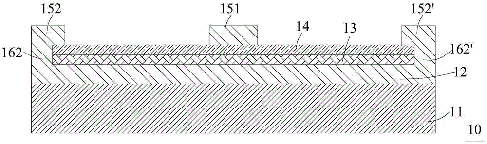
[0029] figure 1 It is a cross-sectional view of the field effect diode according to the first embodiment of the present invention. Such as figure 1 As shown, the field effect diode 10 includes a glass substrate 11, an indium tin oxide conductive layer 12, an aluminum oxide insulating layer 13, a zinc oxide channel layer 14, and a first electrode located on the zinc oxide channel layer 14, from bottom to top. 151 and second electrodes 152, 152' arranged on opposite sides of the first electrode 151, and conductive pillars 162, 162' contacting two opposite sides of the aluminum oxide insulating layer 13 and the zinc oxide channel layer 14. The second electrodes 152, 152' are electrically connected to the indium tin oxide conductive layer...


PUM


Abstract

The invention provides a field effect diode, which comprises a conductive layer, an insulating layer, a channel layer, a first electrode and a second electrode, wherein the conductive layer, the insulating layer and the channel layer are sequentially stacked; the first electrode and the second electrode are in contact with the channel layer; and the second electrode is electrically connected with the conductive layer. The field effect diode provided by the invention has a high rectification ratio.

Description

Technical field [0001] The invention relates to the field of semiconductor devices, in particular to a diode. Background technique [0002] Because the band gap width of silicon (1.12eV) and the band gap width of germanium (0.66eV) are small, PN junction diodes and Schottky junction diodes made of silicon and germanium have poor endurance performance, that is, under high temperature and high temperature. Performance degradation may occur when working under voltage, high current, or light conditions. [0003] In order to improve the withstand performance of the diode, a wide band gap (ie, band gap greater than 2eV) semiconductor is usually used to prepare the diode, for example, SiC with a band gap of 3.2 eV, GaN with a band gap of 3.4 eV or ZnO with a band gap of 3.4 eV are selected. However, wide band gap semiconductors are difficult to be used as N-type and P-type materials at the same time, so homogeneous PN junction diodes cannot be fabricated. The heterogeneous PN junction h...

Claims


Application Information

Patent Timeline
IPC IPC(8): H01L29/87H01L29/417
CPCH01L29/87H01L29/41716
Inventor 张永晖梅增霞梁会力杜小龙
Owner INST OF PHYSICS - CHINESE ACAD OF SCI
Why Eureka
Try Eureka