High-In-composition InGaN/GaN quantum well structure solar cell based on self-supporting GaN substrate and preparation method thereof

A solar cell, self-supporting technology, applied in circuits, photovoltaic power generation, electrical components, etc., can solve the problems of high defect density, high In composition and high quality, and it is difficult to obtain high-quality high In composition InGaN thin films, etc. Efficiency, the effect of expanding the light absorption range

Active Publication Date: 2016-05-04
江苏第三代半导体研究院有限公司
View PDF4 Cites 2 Cited by
  • Summary
  • Abstract
  • Description
  • Claims
  • Application Information

AI Technical Summary

Problems solved by technology

However, the current InGaN materials have the problems of large defect density and high-quality high-In composition, and it is difficult to obtain high-quality InGaN films with high-In composition

Method used


Image

  • High-In-composition InGaN/GaN quantum well structure solar cell based on self-supporting GaN substrate and preparation method thereof

Examples


Embodiment 1

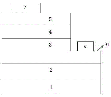
[0034] A self-supporting GaN substrate 1, the substrate is gallium nitride material, the size of the gallium nitride self-supporting wafer used is 20.0mm×20.5mm (±0.2mm), the thickness is 350±25μm, and the crystal orientation It is C-plane(0001)±1 0 , TTV≤15μm, bending degree BOW≤20μm, conductivity type is N type, resistivity 5 cm -2 , effective area>90%. The use of gallium nitride substrates can reduce the lattice mismatch and thermal mismatch between the substrate and the epitaxial layer.

[0035] A GaN buffer layer 2, the gallium nitride buffer layer is fabricated on the self-supporting GaN substrate 1, the GaN buffer layer is grown by RF-MBE method, the growth temperature is 500°C, the thickness is 20nm, the gallium nitride buffer layer Layer 2 provides nucleation centers for the subsequent growth of n-type doped GaN layer materials.

[0036] An n-type doped GaN layer 3, the n-type doped GaN layer 3 is fabricated on the gallium nitride buffer layer 2, and the doped GaN ...

Embodiment 2

[0043] A self-supporting GaN substrate 1, the substrate is gallium nitride material, the size of the gallium nitride self-supporting wafer used is 20.0mm×20.5mm (±0.2mm), the thickness is 350±25μm, and the crystal orientation is C-plane(0001)±1 0 , TTV≤15μm, bending degree BOW≤20μm, conductivity type is N type, resistivity 5 cm -2 , effective area>90%. The use of gallium nitride substrates can reduce the lattice mismatch and thermal mismatch between the substrate and the epitaxial layer.

[0044] A GaN buffer layer 2, the gallium nitride buffer layer is fabricated on the self-supporting GaN substrate 1, the GaN buffer layer is grown by RF-MBE method, the growth temperature is 500°C, the thickness is 15nm, the gallium nitride buffer layer Layer 2 provides nucleation centers for the subsequent growth of n-type doped GaN layer materials.

[0045] An n-type doped GaN layer 3, the n-type doped GaN layer 3 is fabricated on the gallium nitride buffer layer 2, and the doped GaN buf...


PUM

PropertyMeasurementUnit
Thicknessaaaaaaaaaa
Thicknessaaaaaaaaaa
Growth thicknessaaaaaaaaaa

Abstract

The invention provides a high-In-composition InGaN / GaN quantum well structure solar cell based on a self-supporting GaN substrate and a preparation method thereof. The solar cell is composed of the self-supporting GaN substrate, a GaN buffer layer, an n-type doped GaN layer, a high-In-composition InGaN / GaN quantum well layer, a p-type doped GaN layer and a P-type electrode which are laminated in turn. An epitaxial layer is grown by adopting the self-supporting GaN substrate, and high In composition is adopted in the quantum well layer; an n-type doped GaN layer mesa is manufactured by adopting a dry etching method, and an N-type electrode is formed on the mesa; and the P-type electrode is formed on the p-type doped GaN layer by adopting the methods of photoetching and film coating. Performance of the solar cell can be greatly enhanced; and crystal lattice mismatching can be effectively reduced by adopting the self-supporting GaN substrate, and high-quality high-In-composition InGaN is grown by adopting an RF-MBE technology so that light absorption range of the solar cell can be greatly enhanced.

Description

technical field [0001] The invention relates to the field of semiconductor device technology and photoelectric devices, in particular to a high In composition InGaN / GaN quantum well structure solar cell based on a self-supporting GaN substrate. Background technique [0002] Solar energy is a clean, non-polluting, inexhaustible new energy source that has incomparable advantages over other new energy sources. An important application of solar energy in today's world is solar cells. A solar cell is a semiconductor device that directly converts solar energy into electrical energy through the principle of photoelectric conversion. At present, silicon-based solar cells are the most mature and have the highest conversion efficiency in the world, but due to their disadvantages of high cost and short life, people have begun to pay close attention to solar cells based on III-nitride compounds. The band gap of group III nitrides can change continuously from 0.7eV to 6.2eV, and the co...

Claims


Application Information

Patent Timeline
IPC IPC(8): H01L31/0304H01L31/0352H01L31/18
CPCH01L31/0304H01L31/03044H01L31/03048H01L31/035236H01L31/1848H01L31/1856Y02E10/544Y02P70/50
Inventor 尹以安刘力章勇张琪伦
Owner 江苏第三代半导体研究院有限公司
Why Eureka
Try Eureka