LED chip electrode structure that can improve lateral current spreading and has double reflective surfaces

A LED chip and electrode structure technology, applied in the direction of circuits, electrical components, semiconductor devices, etc., can solve the problems of poor reflection effect, low reflectivity, and poor light extraction effect, so as to increase light output efficiency and promote Diffusion, increase the effect of lateral diffusion

Active Publication Date: 2018-01-30
XIAMEN CHANGELIGHT CO LTD
View PDF3 Cites 0 Cited by
  • Summary
  • Abstract
  • Description
  • Claims
  • Application Information

AI Technical Summary

Problems solved by technology

[0002] Conventional GaN-LED electrode structures have two structures: Cr / Pt / Au and Cr / Al / Ti / Pt / Ti / Pt / Au. The metal used in the first structure has a low reflectivity to light and is also There is a certain amount of light absorption, so the light-taking effect of the LED is not very good
The second structure adopts single-sided reflection of Al (the bottom of the electrode has a certain reflection effect on light), but the reflection effect on the top and side of the electrode is not good.
In addition, these two electrode structures both adopt a pure metal stacking structure, which has a better conductive effect in the vertical direction (perpendicular to the direction of the electrode structure), which is not conducive to the lateral diffusion of current (parallel to the direction of the electrode structure).

Method used


Image

  • LED chip electrode structure that can improve lateral current spreading and has double reflective surfaces
  • LED chip electrode structure that can improve lateral current spreading and has double reflective surfaces
  • LED chip electrode structure that can improve lateral current spreading and has double reflective surfaces

Examples


Embodiment Construction

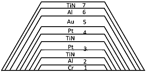
[0021] Such as figure 1 As shown, the present invention includes a layer of Cr layer 1, a first layer of Al 2, a first pair of TiN / Pt layers 3, a second pair of TiN / Pt layers 4, an Au layer 5, The second Al layer 6 and the TiN outer layer 7 constitute the electrode extension bar with trapezoidal structure.

[0022] Wherein, the thickness of the Cr layer is 10-50 angstroms.

[0023] The thickness of the first Al layer is 1000˜5000 angstroms.

[0024] In each pair of TiN / Pt layers, the thickness of TiN is 500-2000 angstroms, and the thickness of Pt is 500-2000 angstroms.

[0025] The thickness of the Au layer is 5000-20000 angstroms.

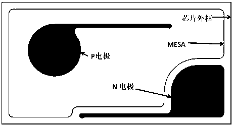
[0026] The electrode structure of the present invention is applied to conventional parallel electrode structure design such as figure 2 shown.

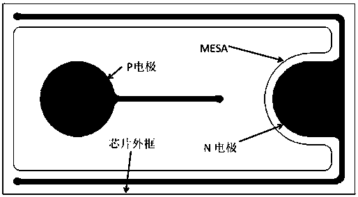
[0027] The electrode structure of the present invention is applied to the design under the situation that the MESA is wrapped by the N electrode extension strip, such as image 3 shown. Its double...


PUM


Abstract

A light emitting diode (LED) chip electrode structure capable of promoting transverse current diffusion and with dual reflection surfaces relates to the technical field of production of an LED chip. The LED chip electrode structure comprises trapezoid structured electrode expansion bars which upwards and sequentially wrap the surface layer of a GaN layer, wherein each trapezoid structured electrode expansion bar comprises a Cr layer, a first Al layer, at least one pair of TiN / Pt layers, an Au layer, a second Al layer and a TiN outer layer. With the electrode structure disclosed by the invention, the transverse current diffusion can be increased, and an effect of multi-surface reflection of light can be achieved.

Description

technical field [0001] The invention relates to the technical field of LED chip production. Background technique [0002] Conventional GaN-LED electrode structures have two structures: Cr / Pt / Au and Cr / Al / Ti / Pt / Ti / Pt / Au. The metal used in the first structure has a low reflectivity to light and is also There is a certain amount of light absorption, so the light-taking effect of the LED is not very good. The second structure uses Al single-sided reflection (the bottom of the electrode has a certain reflection effect on light), but its top and side reflection effects on light are not good. In addition, these two electrode structures both adopt a pure metal stacking structure, which has a better conductive effect in the longitudinal direction (perpendicular to the direction of the electrode structure), and is not conducive to the lateral diffusion of current (parallel to the direction of the electrode). Contents of the invention [0003] The purpose of the present invention i...

Claims


Application Information

Patent Timeline
Patent Type & Authority Patents(China)
IPC IPC(8): H01L33/40
CPCH01L33/405
Inventor 陈亮李俊贤吴奇隆魏振东刘英策李小平邬新根黄新茂蔡立鹤吕奇孟陈凯轩张永林志伟姜伟卓祥景方天足
Owner XIAMEN CHANGELIGHT CO LTD
Why Eureka
Try Eureka