Transmission electron microscope electron diffraction CCD imaging device

An electron microscope and electron diffraction technology, applied in circuits, discharge tubes, electrical components, etc., to save costs and protect photosensitive components

Inactive Publication Date: 2016-05-11
RES CENT FOR ECO ENVIRONMENTAL SCI THE CHINESE ACAD OF SCI
View PDF3 Cites 5 Cited by
  • Summary
  • Abstract
  • Description
  • Claims
  • Application Information

AI Technical Summary

Problems solved by technology

It has been reported in the literature that the vacuum degree of the film chamber is controlled by the microcomputer to reduce the influence of the exhaust and noise of the mec

Method used


Image

  • Transmission electron microscope electron diffraction CCD imaging device
  • Transmission electron microscope electron diffraction CCD imaging device

Examples


Embodiment Construction

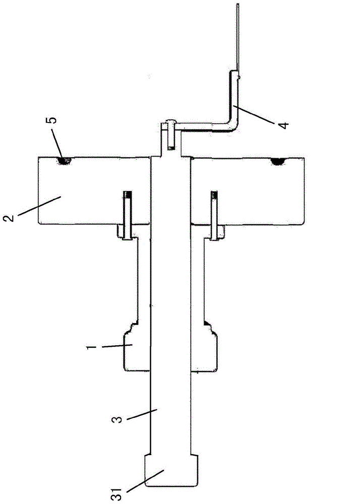
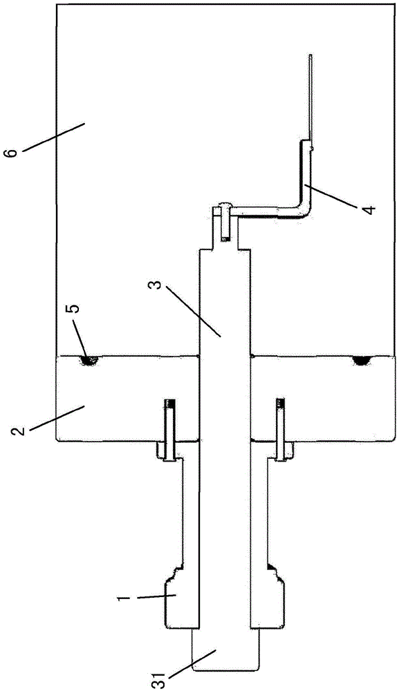
[0022] The electronic diffraction CCD imaging device of the transmission electron microscope of the present invention uses a shielding plate made of copper to shield the excessively strong transmitted light in the electron beam, so as to protect the CCD photosensitive element from being damaged, and the scattered light with the electron diffraction signal is not affected, realizing Electron diffraction CCD imaging of the sample. The electronic diffraction CCD imaging function equipment of the transmission electron microscope of the present invention is mainly aimed at the side-inserted CCD, which solves the problems of cumbersome photographing of electron diffraction imaging negatives and easy loss of data in the past, and also avoids the impact of mechanical pump noise in the negative film room on the resolution of the transmission electron microscope. The impact of the transmission electron microscope electron diffraction CCD imaging function is realized.

[0023] The presen...


PUM


Abstract

The invention relates to a transmission electron microscope electron diffraction CCD imaging device. The transmission electron microscope electron diffraction CCD imaging device comprises a transmission shaft and a protection sleeve; one end of the transmission shaft is an enlarged portion, and the other end of the transmission shaft is connected with a shielding portion; the protection sleeve is fixed at one side surface of a vacuum protection box; a coaxial through hole is formed in the protection sleeve and the vacuum protection box; the transmission shaft is inserted in the through hole of the protection sleeve and the vacuum protection box; the enlarged portion of the transmission shaft is arranged to one side of the protection sleeve; the shielding portion is arranged to one side of the vacuum protection box; the vacuum protection box is connected with the lens barrel of a transmission electron microscope electron; and the shielding portion extends into the transmission electron microscope electron so as to shield a transmission light source. With the transmission electron microscope electron diffraction CCD imaging device of the invention adopted, the problems of complex negative film shooting and high possibility of data loss in existing electron diffraction CCD imaging can be solved, and the influence of the noises of a mechanical pump of a negative film chamber on the resolution of the transmission electron microscope can be avoided, and a transmission electron microscope electron diffraction CCD imaging function can be realized.

Description

technical field [0001] The invention relates to a transmission electron microscope electron diffraction CCD imaging functional device. Background technique [0002] Transmission Electron Microscope (TEM for short), referred to as TEM, is to project the accelerated and concentrated electron beam onto a very thin sample, and the electrons collide with the atoms in the sample to change the direction, thereby producing solid angle scattering (scattering angle The size of the sample is related to the density and thickness of the sample), and can form images with different brightness and darkness, which are finally displayed on imaging devices (such as fluorescent screens, films, and photosensitive coupling components) after zooming in and focusing. [0003] Due to the very short de Broglie wavelength of the electron, the resolution of the transmission electron microscope is much higher than that of the optical microscope, which can reach 0.1-0.2nm, and the magnification is tens o...

Claims


Application Information

Patent Timeline
IPC IPC(8): H01J37/22H01J37/295
Inventor 黎刚张同亮杨永健李洁李红华张庆华
Owner RES CENT FOR ECO ENVIRONMENTAL SCI THE CHINESE ACAD OF SCI
Why Eureka
Try Eureka