
Separate grid type flash memory manufacturing method and separate grid type flash memory

A manufacturing method and technology for separating gates, applied in information storage, static memory, digital memory information and other directions, can solve problems such as structural asymmetry, inconsistent width, and no solution, and achieve improved symmetry, improved performance, and reduced manufacturing. cost effect

Active Publication Date: 2016-05-11
SEMICON MFG INT (SHANGHAI) CORP
View PDF3 Cites 11 Cited by
  • Summary
  • Abstract
  • Description
  • Claims
  • Application Information

AI Technical Summary

Problems solved by technology

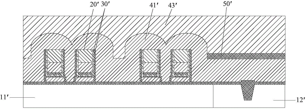
Due to a certain error in the photolithography process (for example, there is an error in the photomask pattern used in the photolithography process), the position defined by the photolithography process to form the word line gate 70 ′ is deviated, and the formed word line The gates 70' (that is, the two word line gates 70' located outside each pair of gate stack structures 20') have inconsistent widths
At the same time, the above manufacturing method requires chemical mechanical polishing of the first polysilicon layer 41' and the second polysilicon layer 43'. However, the chemical mechanical polishing process has the problem of uneven grinding rate, so that the formed word line gate 70' (that is, the heights of the two word line gates 70' located outside each pair of gate stack structures 20') are inconsistent
To sum up, it is difficult to control the feature size of the word line grid 70' formed by the above-mentioned manufacturing method, so that the structure of the formed word line grid 70' is asymmetrical, thereby reducing the performance of the split gate flash memory
For the above problems, there is currently no effective solution

Method used


Image

  • Separate grid type flash memory manufacturing method and separate grid type flash memory
  • Separate grid type flash memory manufacturing method and separate grid type flash memory
  • Separate grid type flash memory manufacturing method and separate grid type flash memory

Examples


Embodiment Construction

[0029] It should be noted that, in the case of no conflict, the embodiments in the present application and the features in the embodiments can be combined with each other. The present application will be described in detail below with reference to the accompanying drawings and embodiments.

[0030]It should be noted that the terminology used here is only for describing specific implementations, and is not intended to limit the exemplary implementations according to the present application. As used herein, unless the context clearly dictates otherwise, the singular is intended to include the plural, and it should also be understood that when the terms "comprising" and / or "comprising" are used in this specification, they mean There are features, steps, operations, means, components and / or combinations thereof.

[0031] For the convenience of description, spatially relative terms may be used here, such as "on ...", "over ...", "on the surface of ...", "above", etc., to describe ...


PUM


Abstract

The invention discloses a separate grid type flash memory manufacturing method and a separate grid type flash memory. The manufacturing method comprises the following steps: providing a semiconductor substrate including a core storage area and a peripheral circuit area, wherein at least one pair of grid lamination structures and sidewall dielectric layers covering the sides of the grid lamination structures are formed in the core storage area; forming a polycrystalline silicon layer covering the grid lamination structures, the sidewall dielectric layers and the exposed surface of the semiconductor substrate; etching the polycrystalline silicon layer in the core storage area in order to form word line grids on the outer side of each pair of grid lamination structures and form an erasable grid between the adjacent sidewall dielectric layers of each pair of grid lamination structures; and etching the polycrystalline silicon layer in the peripheral circuit area to form peripheral grids. According to the manufacturing method, the word line grids are formed through self-alignment, so that the symmetry of the formed word line grids is improved, and the performance of the separate grid type flash memory is improved.

Description

technical field [0001] The present application relates to the technical field of semiconductor integrated circuits, and in particular, to a method for manufacturing a split-gate flash memory and a split-gate flash memory. Background technique [0002] Split-gate flash memory has the advantages of being able to store, read, and erase data multiple times, and the stored data will not disappear after power failure, and has become widely used in personal computers and electronic devices. A non-volatile memory element. Existing split-gate flash memory generally includes a semiconductor base with a core storage area and a peripheral circuit area, at least one pair of gate stack structures disposed on the core storage area, and words disposed outside each pair of gate stack structures. A wire grid, an erasable gate disposed between adjacent sidewall dielectric layers in each pair of gate stack structures, and a peripheral gate disposed in the peripheral circuit area. Wherein, the...

Claims


Application Information

Patent Timeline
IPC IPC(8): H01L21/28H01L21/8247G11C11/34H01L27/11529
Inventor 周侃周儒领
Owner SEMICON MFG INT (SHANGHAI) CORP
Learn More