Color film substrate, display panel and display device

A color film substrate and display panel technology, which is applied in nonlinear optics, instruments, optics, etc., can solve the problems of ITO film mechanical damage and static electricity accumulation, and achieve the effects of reducing static electricity accumulation, improving transmittance, and simplifying the process

Inactive Publication Date: 2016-05-25
BOE TECH GRP CO LTD +1
View PDF5 Cites 34 Cited by
  • Summary
  • Abstract
  • Description
  • Claims
  • Application Information

AI Technical Summary

Problems solved by technology

[0006] The purpose of the present invention is to provide a color filter substrate, a display panel and a display device to solve the problems in the prior art that the ITO film is easily damaged by machinery or the external static electricity enters the display device through the ITO conductive film and causes static electricity accumulation.

Method used


Image

  • Color film substrate, display panel and display device
  • Color film substrate, display panel and display device
  • Color film substrate, display panel and display device

Examples


Embodiment 1

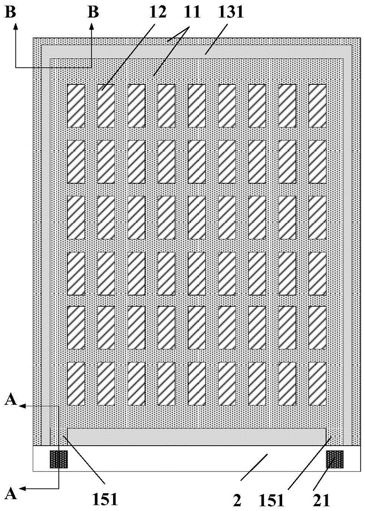
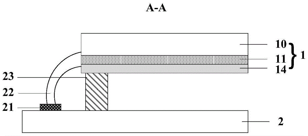
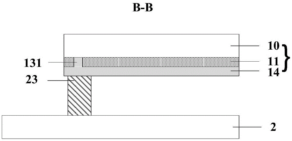
[0034] This embodiment provides a color filter substrate and a display panel including the color filter substrate. figure 1 It is a plan view of the color filter substrate and the display panel of this embodiment. figure 2 It is a cross-sectional view along the A-A direction of the color filter substrate and the display panel of this embodiment. image 3 It is a cross-sectional view of the color filter substrate and the display panel along the B-B direction of this embodiment. The color filter substrate 1 includes a conductive layer located on the color filter side of the color filter substrate, and an isolation strip disposed on a peripheral portion of the conductive layer, and the isolation strip is used to isolate external static electricity.

[0035] In this embodiment, the conductive layer is a black matrix 11 with conductive properties. like figure 1 , 2 As shown in and 3 , the color filter substrate 1 further includes a first substrate 10 and a color filter 12 . T...

Embodiment 2

[0045] This embodiment provides a color filter substrate and a display panel. The difference from Embodiment 1 is that the isolation zone of this embodiment is the first isolation zone 132 extending from the edge of the black matrix of the conductive layer to the edge of the color filter substrate to act as a barrier. Break the role of external static electricity. Figure 4 It is a plan view of the color filter substrate and the display panel of this embodiment. Figure 5 It is a cross-sectional view of the color filter substrate and the display panel along the C-C direction of this embodiment.

[0046] like Figure 4 and Figure 5 As shown, the color filter substrate 1 of this embodiment includes a first substrate 10 , a black matrix 11 , a color filter 12 , and a first isolation zone 132 . The black matrix 11 and the color filter 12 are disposed on the first substrate 10 in the same layer, and the color filter 12 is composed of three color resins of red R, green G and blu...

Embodiment 3

[0049] This embodiment provides a color filter substrate and a display panel. The difference from Embodiment 1 is that the black matrix in this embodiment is a non-conductive conventional black matrix, and the conductive layer is a transparent layer arranged on the color filter side of the color filter substrate. For the conductive layer 16 , the isolation zone is a second isolation groove 133 disposed on the peripheral portion of the transparent conductive layer 16 and dividing the transparent conductive layer into two parts, inner and outer. Image 6 It is a plan view of the color filter substrate and the display panel of this embodiment. Figure 7 It is a cross-sectional view along the D-D direction of the color filter substrate and the display panel of this embodiment. Figure 8 It is a cross-sectional view of the color filter substrate and the display panel along the E-E direction of this embodiment.

[0050] like Image 6 , 7 As shown in and 8 , the color filter subst...


PUM

PropertyMeasurementUnit
surface resistanceaaaaaaaaaa

Abstract

The invention belongs to the technical field of display, and particularly relates to a color film substrate, a display panel and a display device, wherein the color film substrate comprises a conducting layer positioned at the color film side of the color film substrate; an isolation belt used for isolating external static electricity is arranged on the periphery of the conducting layer; a notch is formed in the isolation belt; extending parts used for outputting static electricity are arranged on the inner side conducting layer on the inner sides of the isolation belt; the extending parts extend to the edge of the color film substrate through the notch. According to the color film substrate, the display panel and the display device, the conducting layer and the isolation belt are arranged at the color film side of the color film substrate, so that the problem in the prior art of static electricity accumulation due to external static electricity's entry into the display device through an ITO thin film prone to mechanical damage is effectively solved.

Description

technical field [0001] The invention belongs to the field of display technology, and in particular relates to a color filter substrate, a display panel and a display device. Background technique [0002] Electrostatic Discharge (ESD for short) will occur rapidly with extremely high intensity, break down semiconductor devices, or generate enough heat to melt semiconductor devices, causing damage and scrapping of some components and bringing great economic losses. [0003] During the manufacturing, production, assembly, testing, etc. of the display device, static electricity is easily generated on the display device due to friction, or external static electricity in the air, human body or other charged objects will be transferred to the display device due to electrical connection. When the static electricity on the surface of the substrate accumulates for a long time, electrostatic discharge will occur, and the film layer on the substrate will be broken down, thereby damaging ...

Claims


Application Information

Patent Timeline
Patent Type & Authority Applications(China)
IPC IPC(8): G02F1/1335
CPCG02F1/133514G02F1/133512G02F1/1339G02F2202/22
Inventor 蒋昆王建张瑞辰赵伟李娜宋雪超王春雷
Owner BOE TECH GRP CO LTD
Why Eureka
Try Eureka