Optical fingerprint sensor, and manufacturing method and fingerprint acquisition method thereof

A technology of a fingerprint sensor and a manufacturing method, which are applied in the directions of acquiring/arranging fingerprints/palmprints, printing image collection, instruments, etc., can solve the problems that the structure of the optical fingerprint sensor needs to be improved, etc.

Inactive Publication Date: 2016-05-25
SHANGHAI OXI TECH
View PDF4 Cites 18 Cited by
  • Summary
  • Abstract
  • Description
  • Claims
  • Application Information

AI Technical Summary

Problems solved by technology

[0005] Among the existing optical fingerprint sensor modules, the

Method used


Image

  • Optical fingerprint sensor, and manufacturing method and fingerprint acquisition method thereof
  • Optical fingerprint sensor, and manufacturing method and fingerprint acquisition method thereof
  • Optical fingerprint sensor, and manufacturing method and fingerprint acquisition method thereof

Examples


Embodiment Construction

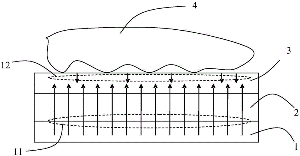
[0058] Since the optical fingerprint sensor requires a relatively high resolution, generally as high as 500dpi (dots per inch, dots per inch), the distance between the data lines in the optical fingerprint sensor is relatively small. In existing optical fingerprint sensors, the distance between adjacent data lines is only about 50 μm or even smaller. Such a small distance can easily cause poor bonding between the chip and the printed circuit board.

[0059] In an existing optical fingerprint sensor, a flexible printed circuit board (Flexible Printed Circuit, FPC) is bound by a film on glass process (Film On Glass, FOG). When the distance between the data lines is only about 50 μm or even smaller, in the process of flexible printed circuit board bonding, the problem of binding alignment deviation is very likely to occur. The alignment deviation of FOG is very large, resulting in flexible printed circuit board binding. The probability of failure is further increased. At the sam...


PUM


Abstract

The invention discloses an optical fingerprint sensor, and a manufacturing method and fingerprint acquisition method thereof. The optical fingerprint sensor comprises a pixel array zone which is disposed on the surface of a substrate and comprises multiple pixels, and multiple scanning lines; the optical fingerprint sensor further comprises a data line gating zone which is disposed on the surface of the substrate, is disposed between the pixel array zone and a binding zone and is internally provided with M gating switches; and the optical fingerprint sensor also comprises M data lines which extend from the pixel array zone to the data line gating zone. In the data line gating zone, in a first direction, every continuous adjacent n data lines form a data line group, n is an integer greater than one, and M is an integer greater than n; in each data line group, one data line and the input end of one gating switch are in one-to-one corresponding connection; and in each data line group, output ends of all the gating switches are connected with one output pin of the binding zone. The optical fingerprint sensor provided by the invention is structurally optimized and is higher in performance.

Description

technical field [0001] The invention relates to the field of optical fingerprint identification, in particular to an optical fingerprint sensor, a manufacturing method thereof, and a fingerprint collection method. Background technique [0002] Fingerprint imaging recognition technology is to collect the fingerprint image of the human body through the optical fingerprint sensor, and then compare it with the existing fingerprint imaging information in the system to judge whether it is correct or not, and then realize the technology of identity recognition. Due to its ease of use and the uniqueness of human fingerprints, fingerprint recognition technology has been widely used in various fields. For example, security inspection areas such as public security bureaus and customs, building access control systems, and consumer products such as personal computers and mobile phones, etc. Fingerprint imaging technology is implemented in various ways such as optical imaging, capacitive...

Claims


Application Information

Patent Timeline
IPC IPC(8): G06K9/00
CPCG06V40/1318
Inventor 凌严朱虹
Owner SHANGHAI OXI TECH
Why Eureka
Try Eureka