

Single-wafer wet cleaning method
A wet-cleaning, monolithic technology, applied in electrical components, semiconductor/solid-state device manufacturing, circuits, etc., can solve problems such as high aspect ratio structure residues
- Summary
- Abstract
- Description
- Claims
- Application Information
AI Technical Summary
Problems solved by technology
Method used
Image

Examples
no. 1 example
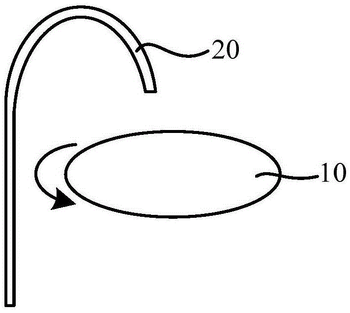
[0037] see image 3 The first embodiment of the present invention is specifically described, wherein, image 3 It is a flow chart of the single-chip wet cleaning method according to the first embodiment of the present invention. In the present invention, the turbulence of the cleaning liquid on the wafer is improved by changing the rotation speed of the wafer.
[0038] The single-chip wet cleaning method is used to clean the wafer, and can be applied to various single-chip wet cleaning processes in semiconductor manufacturing technology, such as cleaning after dry etching, cleaning after planarization, polymerization, etc. Material peeling, etc., the present invention is described by taking polymer peeling as an example. The process of polymer stripping generally includes SPM cleaning steps, SC1 cleaning steps, and SCN cleaning steps. Generally, between the SPM cleaning steps and the SC1 cleaning steps, between the SC1 cleaning steps and the SCN cleaning steps, and after the...
no. 2 example
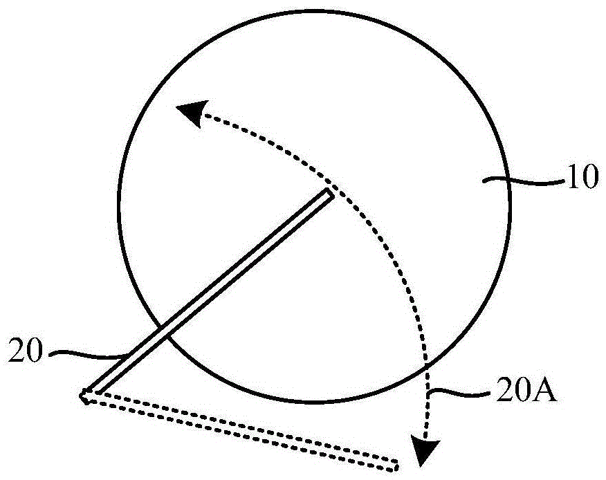
[0052] see Figure 4 The second embodiment of the present invention is specifically described, wherein, Figure 4 It is a flow chart of the single-chip wet cleaning method in the second embodiment of the present invention. In the present invention, the turbulence of the cleaning liquid on the wafer is improved by changing the rotation direction of the wafer.
[0053] In this embodiment, the wafer has two turning directions in the SCI cleaning step. The SCI cleaning step is divided into multiple sub-steps, specifically, refer to Figure 4 , the SCI cleaning step S21 is divided into a plurality of sub-steps: sub-step S211, sub-step S212, sub-step S213, ... sub-step S21n, sub-step S211, sub-step S212, sub-step S213, ... the cleaning solution in sub-step S21n Both are SCI, and the rotation directions of the wafers in at least two of the sub-steps are different.
[0054] Preferably, the rotation directions of the wafer 10 in adjacent sub-steps are all different. Specifically, ...
no. 3 example
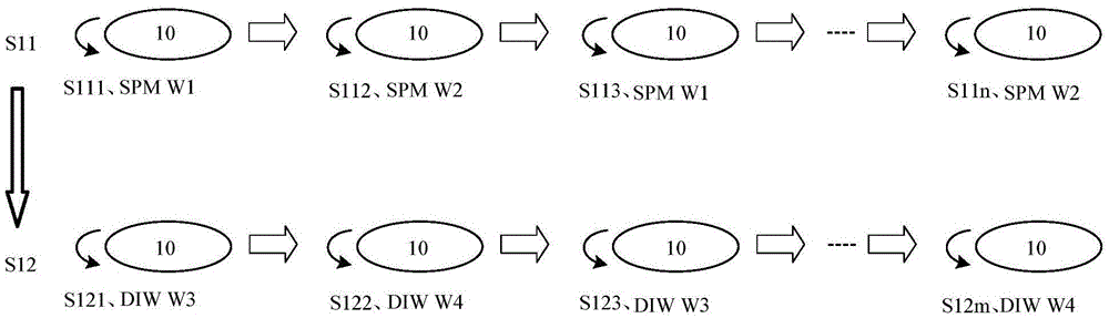
[0064] see Figure 5 The third embodiment of the present invention is specifically described, wherein, Figure 5 It is a flow chart of the single-chip wet cleaning method according to the third embodiment of the present invention. In the present invention, the turbulence of the cleaning liquid on the wafer is improved by changing the rotation speed and rotation direction of the wafer.
[0065] In this embodiment, the wafer has two turning directions in the SCN cleaning step. The SCN cleaning step is divided into multiple sub-steps, specifically, refer to Figure 4 , the SCN cleaning step S31 is divided into a plurality of sub-steps: sub-step S311, sub-step S312, sub-step S313, ... sub-step S31n, sub-step S311, sub-step S312, sub-step S313, ... the cleaning solution in sub-step S31n All are SCN, the rotation speeds of the wafers in some of the sub-steps are different, and the rotation directions of the wafers in some of the sub-steps are different.
[0066] Preferably, the ...
PUM
 Abstract
Description
Claims
Application Information