TFT array substrate structure

An array substrate structure and substrate substrate technology, applied in optics, instruments, electrical components, etc., can solve the problems of reducing the panel aperture ratio, failing to meet high-quality display panels, and small storage capacity of storage capacitors, so as to improve product competition The effect of increasing force, increasing capacity, and improving performance

An array substrate structure and substrate substrate technology, applied in optics, instruments, electrical components, etc., can solve the problems of reducing the panel aperture ratio, failing to meet high-quality display panels, and small storage capacity of storage capacitors, so as to improve product competition The effect of increasing force, increasing capacity, and improving performance

CN105679765AInactive Publication Date: 2016-06-15WUHAN CHINA STAR OPTOELECTRONICS TECH CO LTD

Image

  • TFT array substrate structure
  • TFT array substrate structure

Examples


Embodiment Construction

[0029] In order to further illustrate the technical means adopted by the present invention and its effects, the following describes in detail in conjunction with preferred embodiments of the present invention and accompanying drawings.

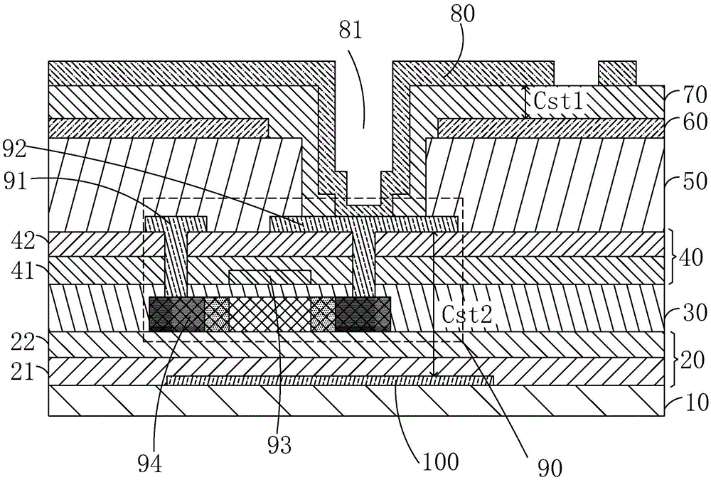
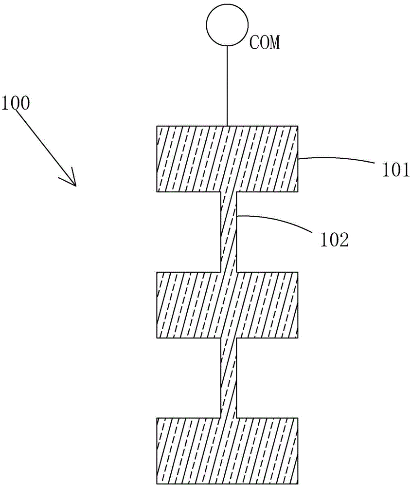
[0030] Please also see figure 1 and figure 2 , the present invention provides a TFT array substrate structure, including: a base substrate 10, a patterned metal light-shielding layer 100 disposed on the base substrate 10, and a first insulating layer covering the patterned metal light-shielding layer 100 20. Several TFTs 90 arranged in an array on the first insulating layer 20, a flat layer 50 covering the TFTs 90, a common electrode 60 arranged on the flat layer 50, and a common electrode covering the The protective layer 70 of 60 and the patterned pixel electrode 80 disposed on the protective layer 70 .

[0031] The TFT 90 includes: a semiconductor layer 94 disposed on the first insulating layer 20 , a gate insulating layer 30 covering th...


PUM


Abstract

The invention provides a TFT array substrate structure. A patterned metal shielding layer (100) comprises a plurality of metal shielding blocks (101) and a metal narrow strip (102), wherein the plurality of metal shielding blocks (101) are arranged in an array form; the metal narrow strip (102) is connected with two adjacent metal shielding blocks (101); the metal shielding layer (100) and a common electrode (60) are connected to a common voltage signal (COM); aiming at each TFT (90), a pixel electrode (80) is in contact with a drain (92) of the TFT (90), so that the opposite overlapping parts of the pixel electrode (80) and the common electrode (60) form a first storage capacitor (Cst1); the opposite overlapping parts of the metal shielding layer (100) and the drain (92) and the pixel electrode (80) form a second storage capacitor (Cst2); the first storage capacitor (Cst1) and the second storage capacitor (Cst2) form a parallel relationship; the capacity of the storage capacitors can be increased; the metal shielding layer (100) is located in a shielding region; and the aperture ratio is not affected by improvement of the metal shielding layer (100).

Description

technical field [0001] The present invention relates to the field of display technology, in particular to a TFT array substrate structure. Background technique [0002] Liquid Crystal Display (LCD) has many advantages such as thin body, power saving, and no radiation, and has been widely used, such as: LCD TV, mobile phone, personal digital assistant (PDA), digital camera, computer screen or notebook computer Screens, etc., dominate the field of flat panel displays. [0003] Most of the liquid crystal displays currently on the market are backlight liquid crystal displays, which include a liquid crystal display panel and a backlight module. The working principle of the liquid crystal display panel is to pour liquid crystal molecules between the thin film transistor array substrate (ThinFilmTransistorArraySubstrate, TFTArraySubstrate) and the color filter substrate (ColorFilter, CF), and apply a driving voltage on the two substrates to control the rotation of the liquid cryst...

Claims


Application Information

Patent Timeline
15 Jun 2016
Publication
CN105679765A
IPC
H01L27/12; H01L23/552
CPC
H01L23/552; H01L27/1255; G02F1/136209; G02F1/136213; G02F1/134372; H01L27/124; H01L27/1248; H01L29/78633
Inventors
赵瑜; 张占东