Vertical three-dimensional semiconductor device

A semiconductor and device technology, applied in the field of vertical three-dimensional semiconductor devices, can solve problems such as increased power consumption, increased drive current, increased device manufacturing and processing requirements, etc., to reduce voltage, low drain resistance, and reduce the risk of damage and failure Effect

Inactive Publication Date: 2016-06-15
IMEC非营利协会
View PDF10 Cites 10 Cited by
  • Summary
  • Abstract
  • Description
  • Claims
  • Application Information

AI Technical Summary

Problems solved by technology

However, the scaling of the stack not only increases the fabrication and processing requirements of the device, but also results in an increase in the drive current required for device operation
Larger drive currents result in increased power dissipation and risk of device damage or failure

Method used


Image

  • Vertical three-dimensional semiconductor device
  • Vertical three-dimensional semiconductor device
  • Vertical three-dimensional semiconductor device

Examples


Embodiment Construction

[0038]The present invention will now be described more fully hereinafter with reference to the accompanying drawings, in which presently preferred embodiments of the invention are shown. However, this invention may be embodied in many different forms and should not be construed as limited to the embodiments set forth herein. Rather, these embodiments are provided for thoroughness and completeness, and so that they will fully convey the scope of the invention to those skilled in the art.

[0039] It will be understood that the terms "vertical" and "horizontal" are used herein to refer to specific directions as shown in the figures and that these terms are not limitations of the specific embodiments described herein.

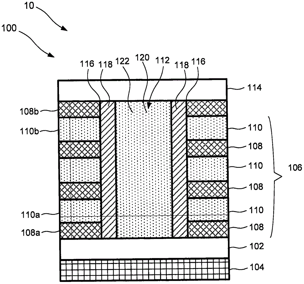
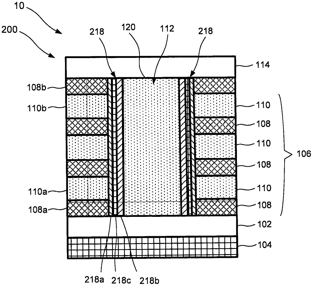
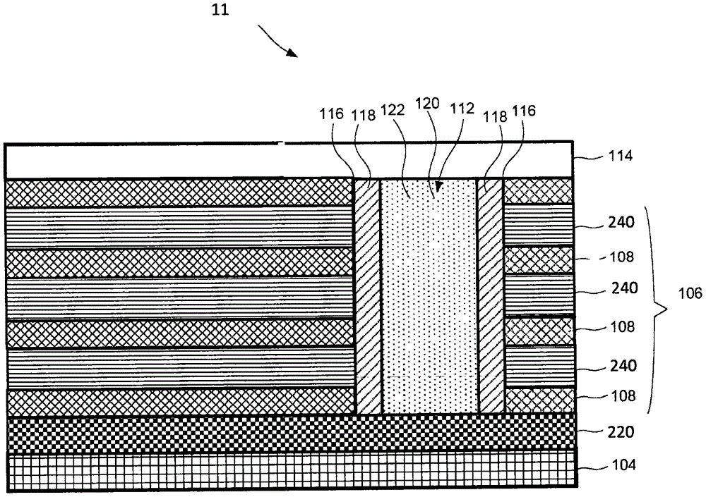
[0040] figure 1 with 2 A cross-sectional view of an initial stage of a vertical three-dimensional semiconductor device 10 is shown. As will be further described below, the vertical three-dimensional semiconductor device 10 is a junctionless device. According t...


PUM


Abstract

The present invention relates to a vertical, three-dimensional semiconductor device (10) comprising a source layer (102) on a substrate (104), a horizontal stack of layers (106) of a repetitive sequence on the source layer (102), each sequence comprising an electrically isolating layer (108) and an electrically conductive gate layer (110). An electrically isolating layer (108a) of the stack of layers (106) is in contact with the source layer (102), a vertical channel structure (112) extending through the horizontal stack of layers (106), a metal drain (114) being arranged above the horizontal stack of layers (106) and the vertical channel structure (112), the source layer (102) being arranged to inject charge carries into the vertical channel structure (112) and the metal drain (114) being arranged to extract charge carries from the vertical channel structure (112). The semiconductor device (10) may be junction-less and the vertical channel structure (112) may comprise a high mobility semiconductor material.

Description

technical field [0001] The present invention relates to a vertical three-dimensional semiconductor device and a method for manufacturing such a device. Background technique [0002] Advances in semiconductor manufacturing and processing technology over the past 50 years have resulted in integrated circuits with consistently smaller physical transistor devices, allowing more circuitry to be packed on a single chip. This increased capacity per unit area typically reduces cost or increases functionality such that the number of transistors in an integrated circuit roughly doubles every two years. As a result, the production of more cost-effective electronic devices that may have increased functionality has been provided over time. In general, as the physical size of transistor devices shrinks, device performance, cost per unit, and switching power consumption decrease while speed increases. [0003] However, transistor scaling has become increasingly difficult over time as the...

Claims


Application Information

Patent Timeline
Patent Type & Authority Applications(China)
IPC IPC(8): H01L29/78H01L21/336
CPCH01L29/66484H01L29/66553H01L29/66666H01L29/7827H01L29/7831H01L29/66833H01L29/7828H01L29/7926H01L29/0638H01L29/20H01L29/22H10B43/27H01L29/16H01L29/161
Inventor 陈青林J(G)·利森尼 雷耶斯
Owner IMEC非营利协会
Why Eureka
Try Eureka