Silicon chip surface height and gradient detection apparatus and method thereof

A silicon wafer surface and detection device technology, applied in the field of lithography machines, can solve the problems of difficult use, complex optical path design, and uneven reflectivity of silicon wafers, so as to increase process applicability, improve energy utilization, and eliminate silicon The effect of the influence of the underlying pattern on the slice

Active Publication Date: 2016-06-22
SHANGHAI MICRO ELECTRONICS EQUIP (GRP) CO LTD
View PDF8 Cites 7 Cited by
  • Summary
  • Abstract
  • Description
  • Claims
  • Application Information

AI Technical Summary

Problems solved by technology

However, the above method needs to add an additional imaging unit, the optical path design is complex, and the imaging unit’s detector response speed, sensitivity, and timeliness for feedback compensation are high, so it is difficult to use in engineering
[0005] Aiming at the above problems, a detection method based on polarization modulation was proposed later, which optically solves the problem of uneven reflectivity of silicon wafers
However, this automatic focusing and leveling system is only suitable for laser or single-wavelength illumination, and can only detect one wavelength at a time. When multiple wavelengths need to be detected, the detection light source needs to be replaced many times, which increases the complexity of detection and reduces The utilization rate of light source energy and the process applicability of the focus and leveling system to different silicon wafers

Method used


Image

  • Silicon chip surface height and gradient detection apparatus and method thereof
  • Silicon chip surface height and gradient detection apparatus and method thereof
  • Silicon chip surface height and gradient detection apparatus and method thereof

Examples


Embodiment Construction

[0028] Below in conjunction with accompanying drawing, invention is described in detail:

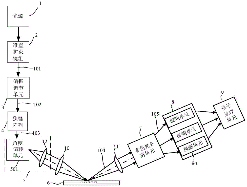
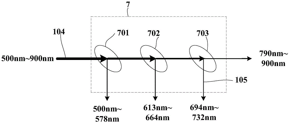
[0029] Such as figure 1 As shown, the present invention provides a silicon wafer surface height and inclination detection device, which includes a light source 1, a collimator beam expander 2, a slit array 4, an angle adjustment unit 5, and a detector 8 arranged in sequence from the detection light path And signal processing unit 9, also includes polarization modulation unit 3 and polychromatic light separation unit 7, described detector 8 is made up of several detection units 80;

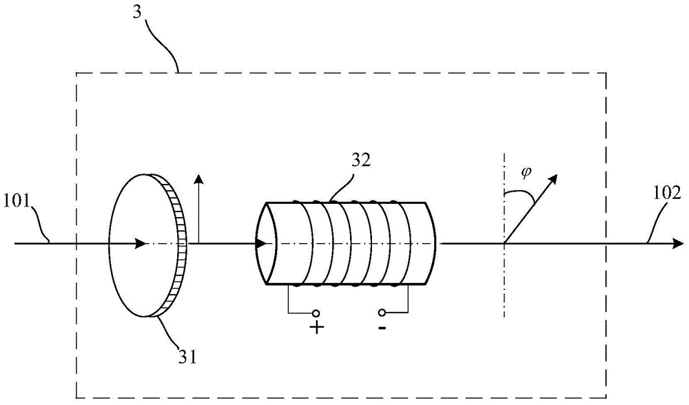
[0030] Specifically, the light source 1 provides an illuminating beam 101, and the illuminating beam 101 sequentially passes through the collimating beam expander 2 used to shape and homogenize the beam to generate a parallel beam, and is used to adjust the polarization direction of the illuminating beam 101. The polarization adjustment unit 3, the slit array 4 for converting the polarized beam 102 into the ...


PUM


Abstract

The invention discloses a silicon chip surface height and gradient detection apparatus and a method thereof. The detection apparatus comprises a light source, a collimating beam expander, a slit array, an angle adjusting unit, a first lens, a silicon chip to be detected, a second lens, a detector and a signal processing unit which are sequentially arranged from a detection light path, and also comprises a polarization modulation unit positioned between the collimating beam expander and the slit array, and a polychromatic light separating unit positioned between the second lens and the detector, and the detector is composed of a plurality of detection units. The polychromatic light separating unit arranged in the invention separates broadband reflected lights into independent wavebands, all the wavebands are individually detected through the corresponding detection units, and detection information of all the wavebands is comprehensively processed to well eliminate the influences of the bottom layer pattern of the silicon chip in order to obtain accurate silicon chip surface position information; and the broadband light source is used, so the light source energy utilization rate is improved, and the processing suitability of the detection apparatus to different silicon chips is improved.

Description

technical field [0001] The invention relates to the technical field of photolithography machines, in particular to a device and method for detecting the height and inclination of a silicon wafer surface. Background technique [0002] A projection lithography machine is a device that projects the pattern on the mask onto the surface of a silicon wafer through a projection objective lens. During the exposure process of the lithography machine, if the defocus or inclination of the silicon wafer relative to the focal plane of the objective lens makes some areas in the exposure field of view outside the effective glue depth, it will seriously affect the quality of lithography, so focus adjustment must be used The flat system is precisely controlled. The general working principle of the existing focusing and leveling system is: first obtain the information of the surface height and inclination of the silicon wafer in the entire exposure field, so as to judge whether the automatic...

Claims


Application Information

Patent Timeline
Patent Type & Authority Applications(China)
IPC IPC(8): G03F7/20
Inventor 张鹏黎徐文王帆
Owner SHANGHAI MICRO ELECTRONICS EQUIP (GRP) CO LTD
Why Eureka
Try Eureka