An integrated structure of an LDMOS and a JFET and a manufacturing method thereof

A technology of channel region and field oxide layer, applied in semiconductor/solid-state device manufacturing, electrical components, electric solid-state devices, etc., can solve problems such as high-voltage LDMOS reliability problems

Active Publication Date: 2016-06-22
SHANGHAI HUAHONG GRACE SEMICON MFG CORP
View PDF4 Cites 4 Cited by
  • Summary
  • Abstract
  • Description
  • Claims
  • Application Information

AI Technical Summary

Problems solved by technology

[0024] The JFET and LDMOS of the above-mentioned existing structure share the drift region and the drain region, which can realize the high durability of the JFET, but the disadvantage is that the gate region of the JFET and the channel region of the LDMOS share the P well 105a, an

Method used


Image

  • An integrated structure of an LDMOS and a JFET and a manufacturing method thereof
  • An integrated structure of an LDMOS and a JFET and a manufacturing method thereof
  • An integrated structure of an LDMOS and a JFET and a manufacturing method thereof

Examples


Embodiment Construction

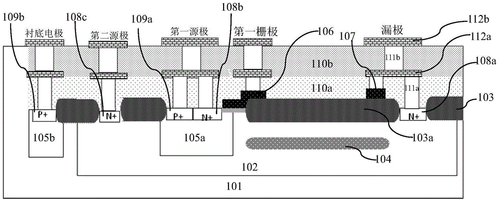
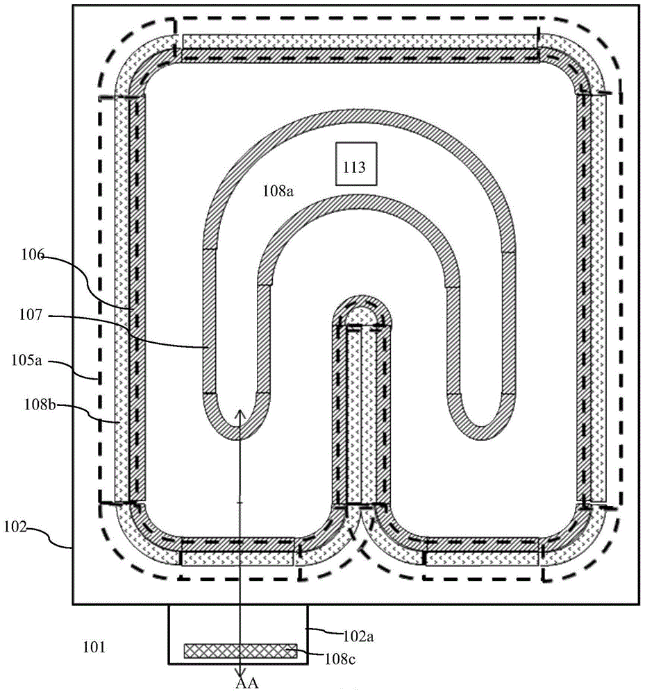
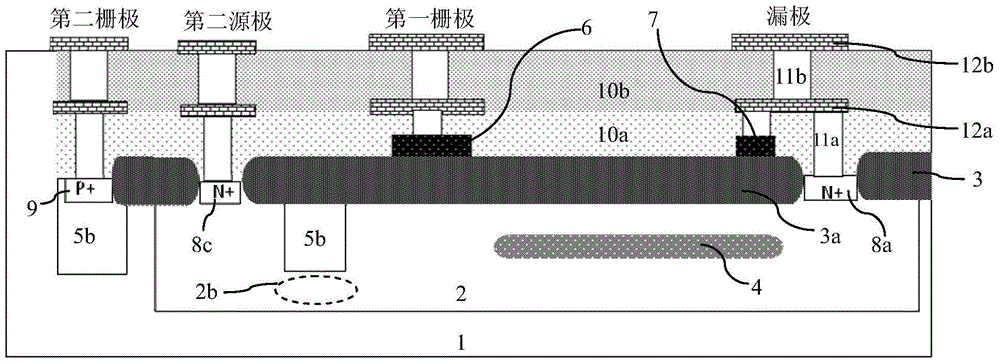
[0113] like image 3 Shown is the sectional view of JFET in the integrated structure of LDMOS and JFET of the embodiment of the present invention; Figure 4 Shown is a top view of the integrated structure of LDMOS and JFET according to the embodiment of the present invention. In the integrated structure of the embodiment of the present invention LDMOS and JFET:

[0114] LDMOS includes:

[0115] The deep N well 2 is formed in the P-type substrate 1, and the field oxide layer 3 is formed in the P-type substrate 1, and the active region is isolated by the field oxide layer 3.

[0116] The first channel region 5a (please refer to Figure 4 shown), consisting of a P well formed in the deep N well 2.

[0117] The first source region 8b (please refer to Figure 4 shown), consisting of N+ regions formed in the first channel region 5a.

[0118] The first drain region 8 a is composed of an N+ region formed in the deep N well 2 .

[0119] A field oxide layer 3 is formed on the sur...


PUM

PropertyMeasurementUnit
Distanceaaaaaaaaaa
Distanceaaaaaaaaaa

Abstract

The invention discloses an integrated structure of an LDMOS and a JFET and a manufacturing method thereof. The JFET uses a drift region and a drain region, which are also the drift region and the drain region of the LDMOS. A first polysilicon layer is connected in an end to end mode to form a closed first polysilicon encircling structure. A source region and a channel region of the LDMOS respectively circle around the outer side of the first polysilicon layer to form a source region encircling structure with an opening. A gate electrode region and a source region of the JFET form in a deep N-well outside an opening position, so that a gate electrode region of the JFET and the channel region of the LDMOS are separated. The invention also discloses a manufacturing method for the integrated structure of the LDMOS and the JFET. According to the invention, high-voltage resistance of the JFET can be realized; meanwhile, the reliability of the LDMOS device can be raised; and relatively low cost is realized.

Description

technical field [0001] The invention relates to the field of semiconductor integrated circuit manufacturing, in particular to a junction field effect transistor (JFET) device. The invention also relates to a manufacturing method of the JFET device. Background technique [0002] In the current high-voltage BCD process, the commonly used method of high-voltage LDMOS with high-voltage JFET is to use the structure of high-voltage LDMOS to provide withstand voltage, and then draw the source region (Source) of JFET at the other end of the high-voltage N well (HVNwell) to form a high-voltage JFET device. [0003] By using the drift region of the isolated high-voltage LDMOS as the drain region or the source region (Drain / Source) of the JFET, and using the body region (body) of the LDMOS, that is, the P well (Pwell) of the channel region, as the JFET gate region (Gate), Realize the JFET parasitic in the LDMOS, and realize the high withstand voltage performance of the JFET through th...

Claims


Application Information

Patent Timeline
IPC IPC(8): H01L27/06H01L29/78H01L29/808H01L21/82
CPCH01L21/82H01L27/0617H01L29/7816H01L29/808
Inventor 苗彬彬
Owner SHANGHAI HUAHONG GRACE SEMICON MFG CORP
Why Eureka
Try Eureka