Preparation method of multi-chip parallel illumination module

A lighting module and multi-chip technology, which is applied in the direction of electrical components, electric solid devices, circuits, etc., can solve the problems of poor uniformity, inconsistent height, and the inability to pre-test production efficiency of ordinary integrated parallel chips, so as to achieve consistent uniformity and reduce Difficulty in encapsulation, solving the effect of low encapsulation efficiency

Active Publication Date: 2016-06-29
山东三晶照明科技有限公司
View PDF3 Cites 4 Cited by
  • Summary
  • Abstract
  • Description
  • Claims
  • Application Information

AI Technical Summary

Problems solved by technology

[0006] Aiming at the outstanding light blocking phenomenon of electrode pads in the existing LED production process, the inability to pre-test the screening parameters of ordinary integrated parallel chips, and the low production efficiency, poor uniformity, and inconsistent height of a single LED chip in the packaging production process , the present invention provides a method for preparing a multi-chip parallel lighting module that is convenient for downstream customers to package. Screening parameters can be pre-tested on core particles

Method used


Image

  • Preparation method of multi-chip parallel illumination module
  • Preparation method of multi-chip parallel illumination module
  • Preparation method of multi-chip parallel illumination module

Examples


Embodiment Construction

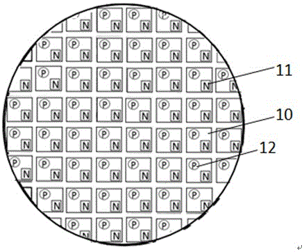
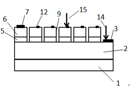
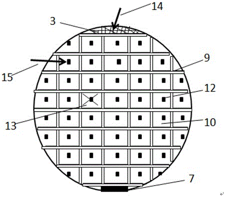
[0037] The multi-chip parallel lighting module of the present invention is prepared by using GaN blue light epitaxial wafers. The structure of the GaN blue light epitaxial wafers includes a sapphire substrate 1, an N-type GaN layer 2, a quantum well active region 5 and a P-type GaN from bottom to top. Layer 6. Concrete preparation method comprises the following steps:

[0038] (1) Preparation of N electrode pad 3

[0039] Such as figure 2 and image 3 As shown, using the existing photolithography mask technology to make an N electrode pattern on one end of the GaN blue epitaxial wafer, and etch from the P-type GaN layer 6 to the N-type GaN layer 2, as the N-electrode pad of the parallel lighting module 3.

[0040] (2) Preparation of electrode pads

[0041] The P electrode pads referred to in this step include the P electrode pads of the entire parallel lighting module (the entire module P electrode pads) and the P electrode pads on the chip unit 10 (chip unit P electrode...


PUM


Abstract

The invention discloses a preparation method of a multi-chip parallel illumination module. The method comprises following steps of (1), preparing N-electrode bonding pads; (2), preparing P-electrode bonding pads; (3), evaporating electrode metal, thus forming a whole module P electrode, chip unit P electrodes and N electrodes; (4), cutting to an N-type GaN layer; (5), testing photoelectric parameters; screening chip units with bad parameters; (6) filling up cutting slots; (7), removing the metal on the surfaces of the chip units; and preparing leads on the whole module P electrode and N electrode, thus obtaining the multi-chip parallel illumination module. According to the method provided by the invention, the packaging difficulty is greatly reduced; the evenness of the chips is consistent; the stability of the packaged chips is improved; the P electrode bonding pads and the N electrode bonding pads on the surfaces of the chip units are removed, therefore, the light shielding area resulting from the connection wires on the bonding pads is reduced; the light-emitting strength of the chips is improved; moreover, in the preparation process, the chip units are tested in advance; the chip particles with bad parameters are eliminated; and the method has actual applicability and operability.

Description

technical field [0001] The invention relates to a preparation method for connecting all chip units or partial chip units in a GaN blue epitaxial wafer in parallel to form a whole to form a multi-chip parallel lighting module, belonging to the technical field of LED chip preparation. Background technique [0002] As the core component of semiconductor lighting, LED chips are faced with increasingly severe market conditions, and higher requirements are put forward for the manufacturing methods of LED chips in terms of how to increase the optical power of chips, improve packaging efficiency, and reduce packaging costs. In traditional LED chips, the P electrodes and N electrodes are set on the surface of the chip, which has a serious light blocking effect. At the same time, most high-power LED chips (such as 5W, 10W, etc.) The pads of the chip are packaged in parallel in a bracket that itself has a circuit structure. This method has high requirements on packaging technology, an...

Claims


Application Information

Patent Timeline
Patent Type & Authority Applications(China)
IPC IPC(8): H01L33/00H01L33/32H01L33/36H01L33/62H01L25/075
CPCH01L25/075H01L33/0075H01L33/32H01L33/36H01L33/62H01L2933/0016H01L2933/0066
Inventor 夏伟曹志芳徐现刚
Owner 山东三晶照明科技有限公司
Why Eureka
Try Eureka