Double split trench gate charge storage type rc-igbt and its manufacturing method

A charge storage and charge storage layer technology, applied in semiconductor/solid-state device manufacturing, circuits, electrical components, etc., can solve the problem of reducing the switching speed of the device, poor reverse recovery characteristics of the freewheeling diode, and affecting the turn-on voltage drop switch of the device. Loss trade-off characteristics, etc.

Active Publication Date: 2018-06-01
UNIV OF ELECTRONICS SCI & TECH OF CHINA
View PDF6 Cites 0 Cited by
  • Summary
  • Abstract
  • Description
  • Claims
  • Application Information

AI Technical Summary

Problems solved by technology

[0004] However, for the traditional RC-CSTBT device structure, in the forward IGBT mode, due to the presence of a higher doping concentration and a certain thickness of the N-type charge storage layer, the breakdown voltage of the device is significantly reduced. In order to effectively shield the N-type Adverse effects of the charge storage layer To obtain a certain device withstand voltage, it is necessary to adopt: 1) deep trench gate depth, so that the depth of the trench gate is greater than the junction depth of the N-type charge storage layer, but the deep trench gate depth not only increases The larger gate-emitter capacitance also increases the gate-collector capacitance, thus reducing the switching speed of the device, increasing the switching loss of the device, and affecting the compromise between the conduction voltage drop and switching loss of the device characteristics; 2) The small cell width minimizes the distance between the trench gates. However, the high-density trench MOS structure not only increases the gate capacitance of the device, but also reduces the switching speed of the device and increases the The switching loss of the device is increased, which affects the compromise characteristics of the conduction voltage drop and switching loss of the device, and increases the saturation current density of the device, making the short-circuit safe working area of ​​the device worse
In the reverse diode freewheeling mode of operation, due to the existence of the built-in potential of the PN junction formed by the P-type base region 7 and the N-type charge storage layer 8 / N-drift region 9, the forward conduction voltage drop is relatively large, and at the same time due to When the freewheeling diode is turned on, a large number of carriers are injected into the N-drift region 9. The existence of a large number of excess carriers makes the reverse recovery characteristics of the freewheeling diode poor, such as long reverse recovery time and large reverse recovery charge. Wait

Method used


Image

  • Double split trench gate charge storage type rc-igbt and its manufacturing method
  • Double split trench gate charge storage type rc-igbt and its manufacturing method
  • Double split trench gate charge storage type rc-igbt and its manufacturing method

Examples


Embodiment 1

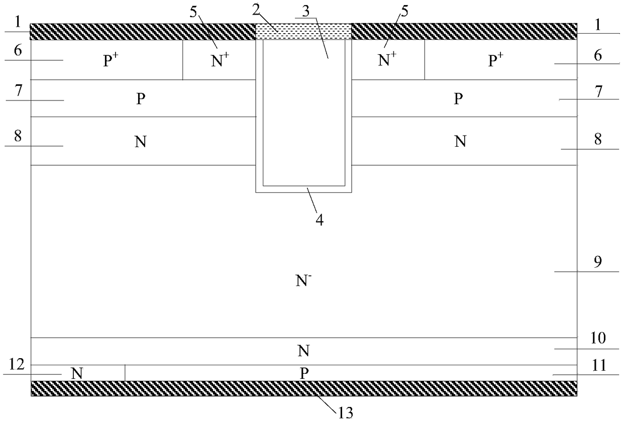
[0051] In this example, a double-split trench gate charge storage RC-IGBT, its cell structure is as follows figure 2 As shown, it includes: the back collector metal 13, the P-type collector region 11 and the N-type collector region 12 located on the back collector metal 13 and connected to it, and the P-type collector region 11 and the N-type collector region The N-type field stop layer 10 above and connected to the N-type field stop layer 10, the N-drift region 9 located on the N-type field stop layer 10 and connected to it; the compound double split trench located in the middle of the upper part of the N-drift region 9 and connected to it Structure; the N-type charge storage layer 8 located on both sides of the upper part of the N-drift region 9 and connected to it, the side wall of the N-type charge storage layer 8 is connected to the side wall of the composite double-split trench structure, located in the N-type charge storage layer The p-type base region 7 on the upper p...

Embodiment 2

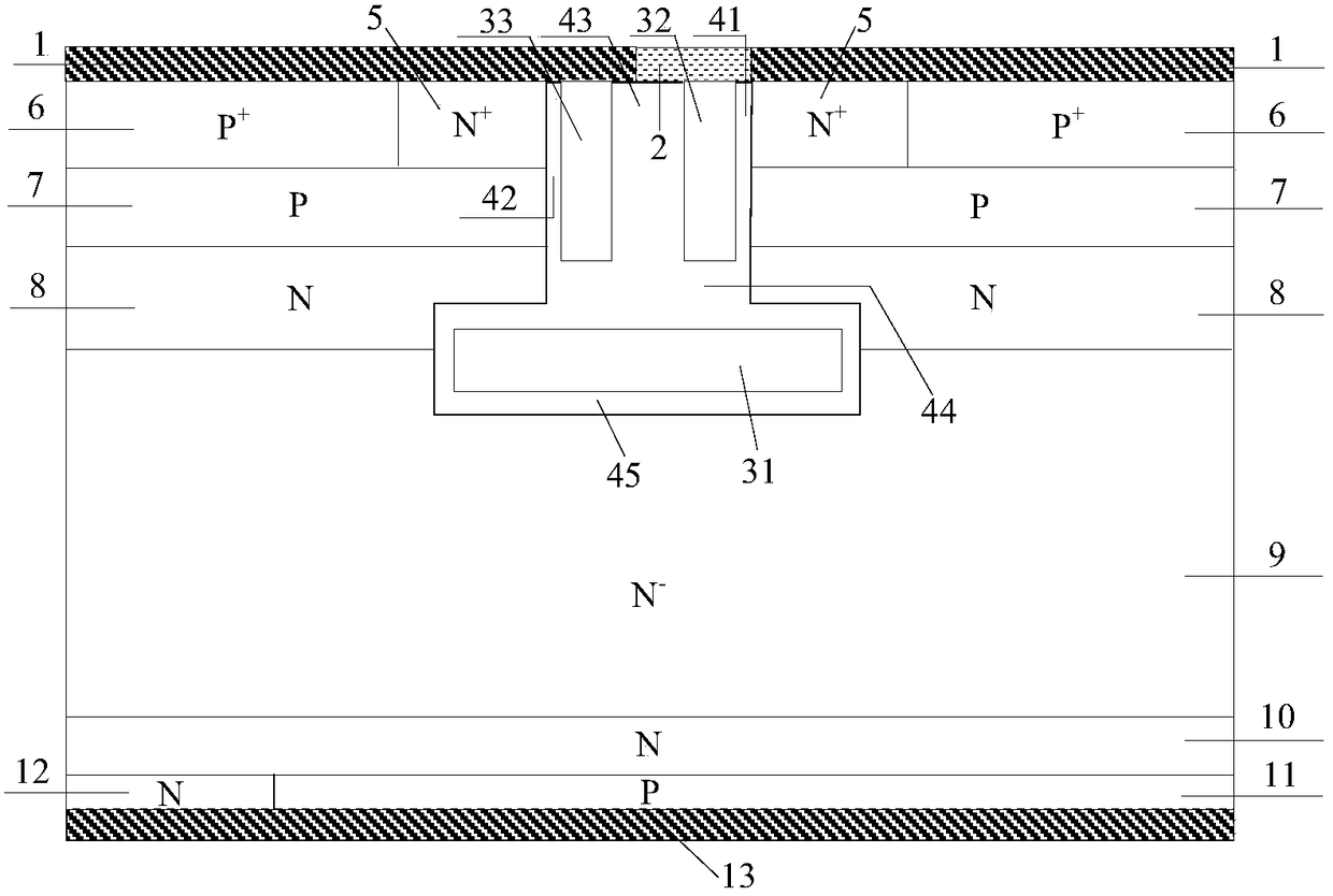
[0053] In this example, a double-split trench gate charge storage RC-IGBT, its cell structure is as follows image 3 As shown, different from Embodiment 1, the lower part of the side split electrode 33 directly extends to the upper surface of the bottom split electrode 31, so that the side split electrode 33 and the bottom split electrode 31 are directly connected to further reduce the gate capacitance of the device.

Embodiment 3

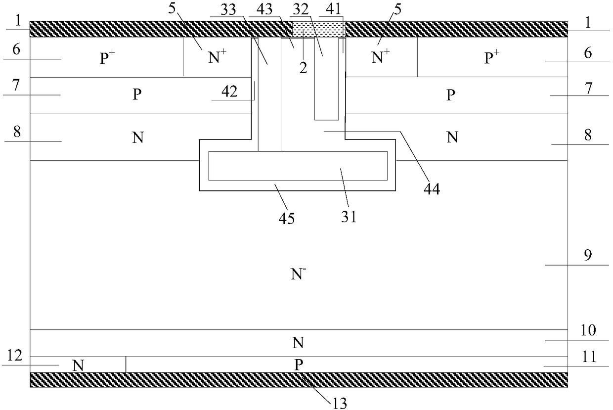
[0055] In this example, a double-split trench gate charge storage RC-IGBT, its cell structure is as follows image 3 As shown, different from Example 1, there is also a layer of N+ layer 14 in the partial region between the underlying structure of the composite trench structure and the p-type base region 7, and the concentration of the N+ layer 14 is higher than that of the N-type The concentration of the charge storage layer 8 and its sidewalls are connected to the composite trench structure, the formed N+ layer 14 further reduces the resistance of the area between the lower layer structure of the composite trench structure and the p-type base region 7, and further improves The carrier injection enhancement effect of the emitter is eliminated, and a better compromise between the forward voltage drop of the device and the switching loss can be obtained.

[0056] The specific implementation scheme of the process manufacturing method of the present invention is described by taki...


PUM


Abstract

The invention belongs to the technical field of power semiconductor devices, and in particular relates to a reverse conduction trench gate charge storage type insulated gate bipolar transistor. The present invention improves the switching of the device in the IGBT working mode by introducing a double-split electrode with the same potential as the emitter and a dielectric layer between the double-split electrode and the gate electrode at the bottom and side surfaces of the gate electrode in the trench of the RC-IGBT device The speed improves the carrier concentration distribution of the entire N-type drift region, reducing the switching loss of the device; reducing the saturation current density of the device, improving the short-circuit safe working area of ​​the device, and improving reliability; When the current diode is in the working mode, the reverse freewheeling diode has a low diode conduction voltage drop, and the reverse recovery characteristics of the freewheeling diode are improved; at the same time, the double split trench gate charge storage type IGBT manufacturing method proposed by the present invention does not Additional process steps are required, which is compatible with traditional RC‑IGBT fabrication methods.

Description

technical field [0001] The invention belongs to the technical field of power semiconductor devices, and relates to an insulated gate bipolar transistor (IGBT), in particular to a reverse conduction trench gate charge storage type insulated gate bipolar transistor (RC-CSTBT). Background technique [0002] Insulated Gate Bipolar Transistor (IGBT) is a new type of power electronic device combining MOS field effect and bipolar transistor. It not only has the advantages of easy driving and simple control of MOSFET, but also has the advantages of low conduction voltage of power transistor, large on-state current and small loss. It has become one of the core electronic components in modern power electronic circuits and is widely used in Various fields of the national economy such as communications, energy, transportation, industry, medicine, household appliances and aerospace. The application of IGBT plays an extremely important role in improving the performance of power electroni...

Claims


Application Information

Patent Timeline
Patent Type & Authority Patents(China)
IPC IPC(8): H01L29/739H01L21/331
CPCH01L29/6634H01L29/7396H01L29/7398
Inventor 张金平廖航刘玮琪刘竞秀李泽宏任敏张波
Owner UNIV OF ELECTRONICS SCI & TECH OF CHINA
Why Eureka
Try Eureka