Silicon-based electro-optic logic AND/NAND gate

An electro-optical and logic technology, applied in the direction of logic circuits using optoelectronic devices, logic circuits using specific components, optics, etc., can solve problems such as low extinction, prone to burrs, and small manufacturing tolerances.

Active Publication Date: 2016-07-13
NINGBO UNIV
View PDF2 Cites 3 Cited by
  • Summary
  • Abstract
  • Description
  • Claims
  • Application Information

AI Technical Summary

Problems solved by technology

However, silicon-based electro-optic logic AND/NAND gates with a microring resonator structure are prone to glitches due to coupling between rings and tuning convers

Method used


Image

  • Silicon-based electro-optic logic AND/NAND gate
  • Silicon-based electro-optic logic AND/NAND gate
  • Silicon-based electro-optic logic AND/NAND gate

Examples


Embodiment 1

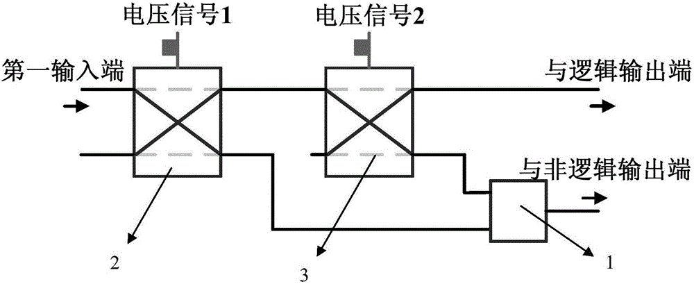
[0017] Embodiment one: if figure 1As shown, a silicon-based electro-optical logic AND / NAND gate includes two 2×2MZI type electro-optic switches with the same structure and a 2×1MMI coupler 1. The 2×2MZI type electro-optic switch has a first input terminal, a second Input terminal, first output terminal and second output terminal, 2×1MMI coupler 1 (multimode interference coupler) has a first input terminal, second input terminal and output terminal, two 2×2MZI type electro-optical with the same structure The switches are respectively the first 2×2MZI type electro-optic switch 2 and the second 2×2MZI type electro-optic switch 3; the first output terminal of the first 2×2MZI type electro-optic switch 2 and the first The input terminal is connected, the first output terminal of the second 2×2MZI type electro-optic switch 3 is an AND logic output terminal, the second output terminal of the second 2×2MZI type electro-optic switch 3 and the first input terminal of the 2×1MMI coupler ...

Embodiment 2

[0019] Embodiment two: if figure 1 As shown, a silicon-based electro-optical logic AND / NAND gate includes two 2×2MZI type electro-optic switches with the same structure and a 2×1MMI coupler 1. The 2×2MZI type electro-optic switch has a first input terminal, a second The input terminal, the first output terminal and the second output terminal, the 2×1MMI coupler 1 has the first input terminal, the second input terminal and the output terminal, and the two 2×2MZI type electro-optical switches with the same structure are respectively the first 2× 2MZI type electro-optic switch 2 and the second 2×2MZI type electro-optic switch 3; the first output end of the first 2×2MZI type electro-optic switch 2 is connected to the first input end of the second 2×2MZI type electro-optic switch 3, and the second 2 The first output end of the × 2MZI type electro-optic switch 3 is connected to the logic output end, the second output end of the second 2 × 2MZI type electro-optic switch 3 is connecte...

Embodiment 3

[0022] Embodiment three: as figure 1 As shown, a silicon-based electro-optical logic AND / NAND gate includes two 2×2MZI type electro-optic switches with the same structure and a 2×1MMI coupler 1. The 2×2MZI type electro-optic switch has a first input terminal, a second The input terminal, the first output terminal and the second output terminal, the 2×1MMI coupler 1 has the first input terminal, the second input terminal and the output terminal, and the two 2×2MZI type electro-optical switches with the same structure are respectively the first 2× 2MZI type electro-optic switch 2 and the second 2×2MZI type electro-optic switch 3; the first output end of the first 2×2MZI type electro-optic switch 2 is connected to the first input end of the second 2×2MZI type electro-optic switch 3, and the second 2 The first output end of the × 2MZI type electro-optic switch 3 is connected to the logic output end, the second output end of the second 2 × 2MZI type electro-optic switch 3 is connec...


PUM

PropertyMeasurementUnit
Thicknessaaaaaaaaaa
Thicknessaaaaaaaaaa
Thicknessaaaaaaaaaa

Abstract

The invention discloses a silicon-based electro-optic logic AND/NAND gate. The silicon-based electro-optic logic AND/NAND gate comprises a first 2*2MZI type electro-optic switch, a second 2*2MZI type electro-optic switch and a 2*1MMI coupler. Each of the first and second 2*2MZI type electro-optic switches comprises a first input end, a second input end, a first output end and a second output end, and the 2*1MMI coupler comprises a first input end, a second input and an output end. The first output end of the first 2*2MZI type electro-optic switch is connected with the first input end of the second 2*2MZI type electro-optic switch, and the first output end of the second 2*2MZI type electro-optic switch is an AND logic output end. The second output end of the second 2*2MZI type electro-optic switch is connected with the first input end of the 2*1MMI coupler, the second output end of the first 2*2MZI type electro-optic switch is connected with the second input end of the 2*1MMI coupler, and the output end of the 2*1MMI coupler is an NAND logic output end. The silicon-based electro-optic logic AND/NAND gate has the advantages of high extinction ratio, high speed, large broadband and large fabrication tolerance.

Description

technical field [0001] The invention relates to a silicon-based optical logic AND / NAND gate, in particular to a silicon-based electro-optical logic AND / AND gate. Background technique [0002] With the rapid increase of the amount of modern information, people have higher and higher requirements for the processor's information processing capability, so most of the existing processors adopt a parallel multi-core structure. How to realize efficient data exchange and processing between cores and between cores and external storage units has become an urgent problem to be solved. Although speed, power consumption and bandwidth limit the application of electrical interconnection in modern high-performance information transmission and processing systems, forming the so-called "electronic bottleneck". However, light is an ideal information carrier with inherent characteristics of high speed, large capacity and parallelism. As the current dominant technology, silicon-based photonics ...

Claims


Application Information

Patent Timeline
IPC IPC(8): G02F3/02H03K19/14
CPCG02F3/022H03K19/14
Inventor 陈伟伟汪鹏君杨甜军周利强张亚伟钱浩宇杨建义
Owner NINGBO UNIV
Why Eureka
Try Eureka