Method for manufacturing thin film transistor

一种薄膜晶体管、制作方法的技术,应用在液晶显示领域,能够解决影响重掺杂漏极区和轻掺杂漏极区电子迁移率、离子均一性影响较大、工艺制备过程复杂等问题,达到避免二次蚀刻、离子均一性小、简化工艺制备过程的效果

Inactive Publication Date: 2016-07-13
WUHAN CHINA STAR OPTOELECTRONICS TECH CO LTD
View PDF4 Cites 3 Cited by
  • Summary
  • Abstract
  • Description
  • Claims
  • Application Information

AI Technical Summary

Problems solved by technology

[0009] The invention provides a method for manufacturing a thin film transistor, which can effectively solve the problem of complicated process preparation and long production cycle in the existing method for manufacturing a thin film transistor, and has a great influence on the uniformity of ions, thereby affecting heavily doped drain regions and Technical Issues of Electron Mobility in Lightly Doped Drain Regions

Method used


Image

  • Method for manufacturing thin film transistor
  • Method for manufacturing thin film transistor
  • Method for manufacturing thin film transistor

Examples


Embodiment Construction

[0031] The following descriptions of the various embodiments refer to the accompanying drawings to illustrate specific embodiments in which the invention may be practiced. The directional terms mentioned in the present invention, such as [top], [bottom], [front], [back], [left], [right], [inside], [outside], [side], etc., are only for reference The orientation of the attached schema. Therefore, the directional terms used are used to illustrate and understand the present invention, but not to limit the present invention. In the figures, structurally similar elements are denoted by the same reference numerals.

[0032] The implementation process of the embodiment of the present invention will be described in detail below in conjunction with the accompanying drawings.

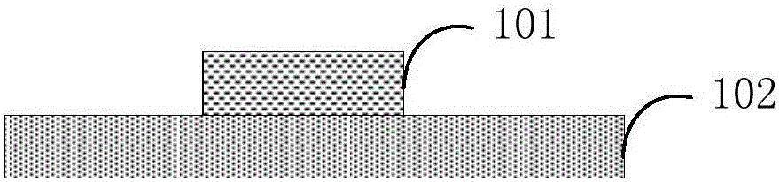
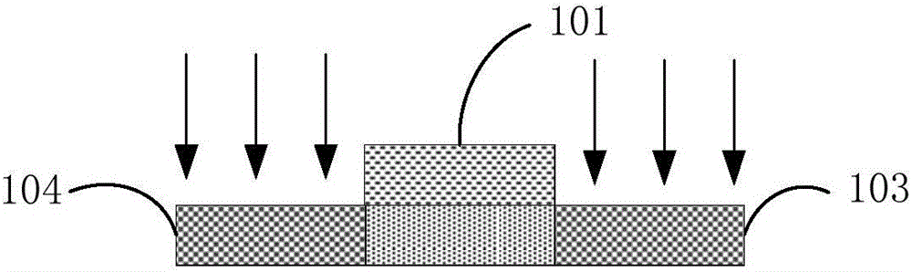
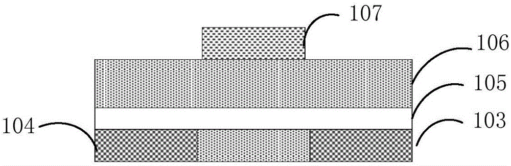
[0033] In view of the complicated preparation process of the thin film transistor, which leads to a long production cycle and is not conducive to production, the following improvements are made.

[0034] like ...


PUM


Abstract

The invention provides a method for manufacturing a thin film transistor. The method comprises the steps of sequentially depositing a gate insulating layer and a gate metal layer on a semiconductor substrate; forming a first photoresistance pattern on the gate metal layer, etching the gate metal layer uncovered with the first photoresistance pattern so as to form a gate electrode, wherein the width of the gate electrode is smaller than that of the first photoresistance pattern; taking the first photoresistance pattern as a mask to perform primary ion implantation on the semiconductor substrate so as to form a preparatory source / drain; etching the side wall of the first photoresistance pattern so as to form a second photoresistance pattern, wherein the width of the second photoresistance pattern is smaller than that of the first photoresistance pattern; taking the second photoresistance pattern as a mask, and performing secondary ion implantation on the semiconductor substrate, so as to form a source / drain, wherein the source / drain comprises a heavy doping drain region and a light doping drain region.

Description

technical field [0001] The invention relates to the technical field of liquid crystal display, in particular to a method for manufacturing a thin film transistor. Background technique [0002] Low-temperature polysilicon panel manufacturing technology is a new generation of thin-film transistor liquid crystal display manufacturing technology. The so-called low-temperature polysilicon technology mainly converts a-Si thin film into polysilicon thin film layer through laser annealing process, and the polysilicon thin film layer is used to form data lines for driving liquid crystal display panels. Thin film transistors of polysilicon and scanning lines, the electron movement speed of polysilicon thin film transistors is a hundred times that of similar amorphous silicon components, so it can realize the characteristics of fast picture response, high brightness display and high resolution of liquid crystal display panels. [0003] like Figure 1A to Figure 1F Shown is the process ...

Claims


Application Information

Patent Timeline
Patent Type & Authority Applications(China)
IPC IPC(8): H01L21/336H01L29/786
CPCH01L29/66765H01L29/78678H01L29/66757H01L29/78621H01L21/26513H01L21/31138H01L21/32135H01L21/32139
Inventor 叶江波
Owner WUHAN CHINA STAR OPTOELECTRONICS TECH CO LTD
Why Eureka
Try Eureka