Method of preventing metal eutectic bonding alloy from overflowing, and device

A eutectic bonding and device technology, which is applied in the direction of electric solid devices, semiconductor devices, metal material coating technology, etc., can solve problems such as device structure failure, MEMS device manufacturing failure, liquid phase alloy 7 overflow, etc.

Active Publication Date: 2016-07-13
INST OF MICROELECTRONICS CHINESE ACAD OF SCI
View PDF5 Cites 11 Cited by
  • Summary
  • Abstract
  • Description
  • Claims
  • Application Information

AI Technical Summary

Problems solved by technology

However, since the two metals that undergo metal eutectic bonding are in contact with each other, the bonding interface diffuses to form a liquid phase alloy 7 with a eutectic composition, and the two metals are combined in a liquid phase eutectic manner, so this There are certain defects in this packaging process, that is, in the process of pressurization and heating, the liquid phase alloy 7 of the eutectic composition will overflow, see Figure 10 , a cross-sectional view of the liquid phase alloy 7 spilling phenomenon after the device silicon wafer 10 and the cap silicon wafer 11 are eutectically bonded
In the absence of a protective structure, the overflowing liquid phase alloy 7 will fall on the device structure area 9, so there is a certain probability that the device structure will fail, resulting in the final failure of the fabrication of the entire MEMS device

Method used


Image

  • Method of preventing metal eutectic bonding alloy from overflowing, and device
  • Method of preventing metal eutectic bonding alloy from overflowing, and device
  • Method of preventing metal eutectic bonding alloy from overflowing, and device

Examples


Embodiment Construction

[0044] In order to make those skilled in the technical field of the present invention understand the present invention more clearly, the technical solutions of the present invention will be described in detail below through specific embodiments in conjunction with the accompanying drawings.

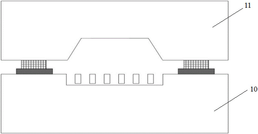
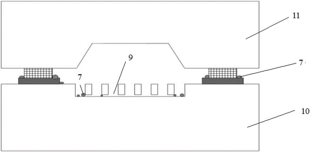
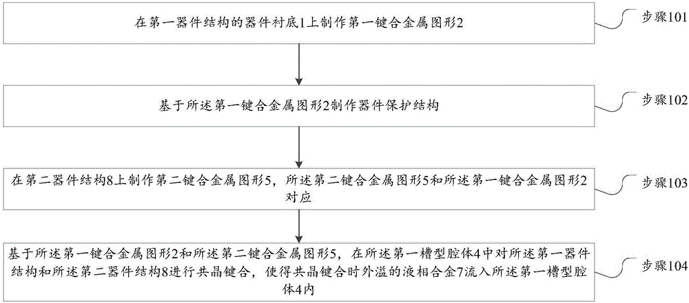
[0045] The embodiment of the invention discloses a method for preventing metal eutectic bonding alloy from overflowing. The method is applied to MEMS device manufacturing and wafer-level vacuum packaging. In this method, a first bonding metal pattern 2 is fabricated on a device substrate 1 of a first device structure, and then a device protection structure is fabricated based on the first bonding metal pattern 2; the device protection structure completely covers the first Bonding the metal pattern 2, and the device protection structure includes a first groove cavity, the bottom surface of the first groove cavity is the first bonding metal pattern 2; and then fabricating on the second devi...


PUM

PropertyMeasurementUnit
angleaaaaaaaaaa

Abstract

The invention discloses a method of preventing a metal eutectic bonding alloy from overflowing. The method comprises the steps of: firstly manufacturing a first bonding metal graph on a device substrate of a first device structure and manufacturing device protecting structure based on the first bonding metal graph, wherein the device protecting structure comprises a first groove-shaped cavity and the bottom of the first groove-shaped cavity is the first bonding metal graph; and then manufacturing a second bonding metal graph on a second device structure and performing metal eutectic bonding on the first device structure and the second device structure in the first groove-shaped cavity. The device protecting structure comprises the first grooved structure, the overflowed liquid alloy can flow into the first groove-shaped cavity in the metal eutectic bonding process, and the overflowed liquid alloy can be obstructed and cannot roll freely, so that the overflowed liquid alloy is effectively prevented from diffusing to the device structure area. According to the invention, the airtight level of the metal bonding is increased, and the yield rate of MEMS device production and manufacturing is improved.

Description

technical field [0001] The invention relates to the technical fields of micro-electro-mechanical system manufacturing and wafer-level vacuum packaging, in particular to a method and a device for preventing metal eutectic bonding alloy from overflowing. Background technique [0002] Bonding refers to the process of closely bonding two substrates of the same or different materials together through physical, chemical or both interactions. [0003] Metal eutectic bonding is a wafer-level vacuum packaging technology that has been widely used in sensors such as accelerometers, gyroscopes, and pressure gauges in recent years, and has become a method for the development and practical application of MEMS (Microelectromechanical Systems, Microelectromechanical Systems) devices. key technologies. Metal eutectic bonding uses a metal layer as an intermediate bonding medium layer, and the two metals are tightly combined by heating and melting to achieve bonding. The so-called eutectic i...

Claims


Application Information

Patent Timeline
Patent Type & Authority Applications(China)
IPC IPC(8): H01L21/60B81C1/00B81B7/02
CPCB81B7/02B81B2201/02B81B2201/0235B81B2201/0242B81B2201/0264B81C1/00261B81C2203/0118H01L24/83H01L2224/83051H01L2924/013
Inventor 云世昌焦斌斌张乐民孔延梅刘瑞文陈大鹏
Owner INST OF MICROELECTRONICS CHINESE ACAD OF SCI
Why Eureka
Try Eureka