Semiconductor made thick photoresist film coating device and application method thereof

A coating device and semiconductor technology, which is applied in the manufacture of semiconductor/solid-state devices, devices for coating liquids on surfaces, spray devices, etc. Thick and uniform, easy to use and flexible, to eliminate the effect of wafer edge protrusion

Active Publication Date: 2016-07-20
SHENYANG KINGSEMI CO LTD
View PDF7 Cites 25 Cited by
  • Summary
  • Abstract
  • Description
  • Claims
  • Application Information

AI Technical Summary

Problems solved by technology

[0002] In the field of semiconductor processing, in the existing spraying photoresist technology, the coating of thick film is processed by spin coating. Because the film is thick, it needs to be coated more than two times and the spreading process is slow. Very low, and the uniformity is difficult to control, and there is a circle of bumps on the edge of the wafer after spin coating, which makes the edge of the wafer unusable and reduces the utilization rate of the product
As semiconductor production refinement and high integration requirements are getting higher and higher, wafer productivity and yield are getting more and more attention. In various processing processes, the treatment of spraying photoresist on the wafer surface is particularly important, especially The optimization of the spraying processing speed on the wafer surface has an important impact on increasing production capacity, reducing costs, and increasing benefits. However, there is an inverse relationship between the spraying speed and the spraying thickness. When the thickness is high, multiple sprayings need to be repeated back and forth, which also greatly increases the time-consuming of single-wafer spraying processing, resulting in a decrease in production capacity

Method used


Image

  • Semiconductor made thick photoresist film coating device and application method thereof
  • Semiconductor made thick photoresist film coating device and application method thereof
  • Semiconductor made thick photoresist film coating device and application method thereof

Examples


Embodiment Construction

[0024] The present invention will be described in further detail below in conjunction with the accompanying drawings.

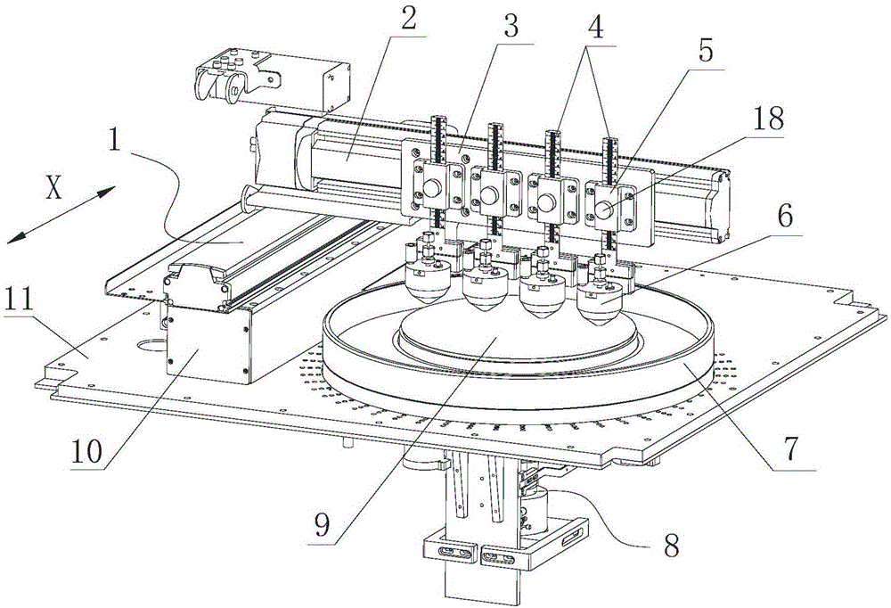
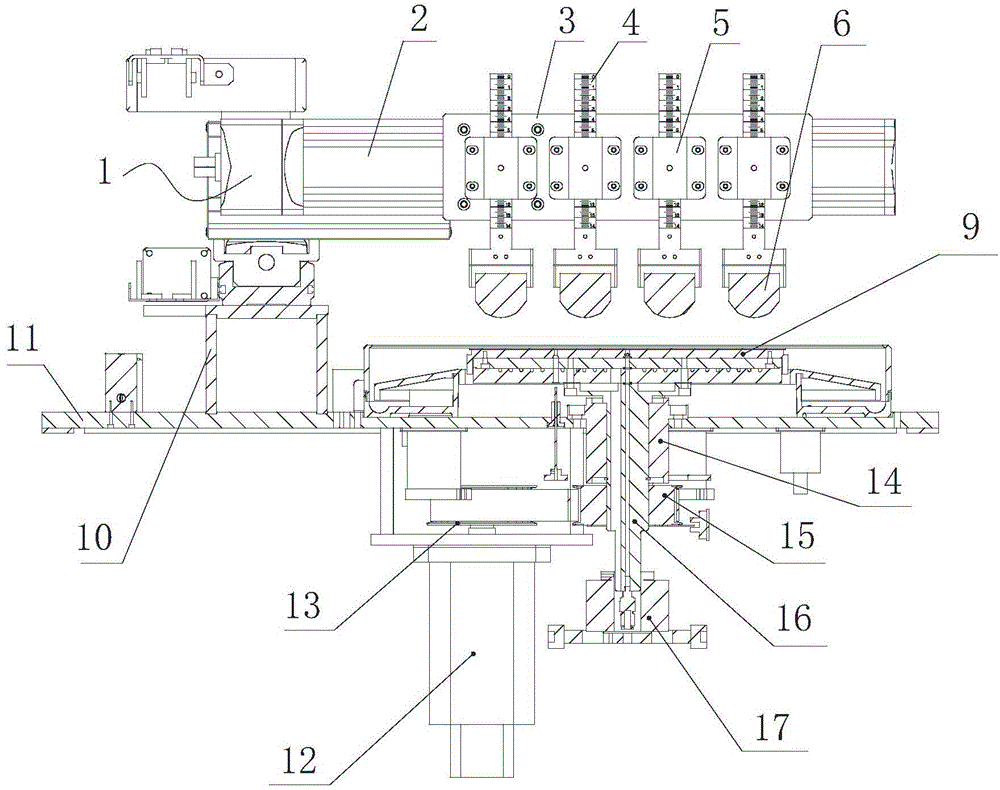
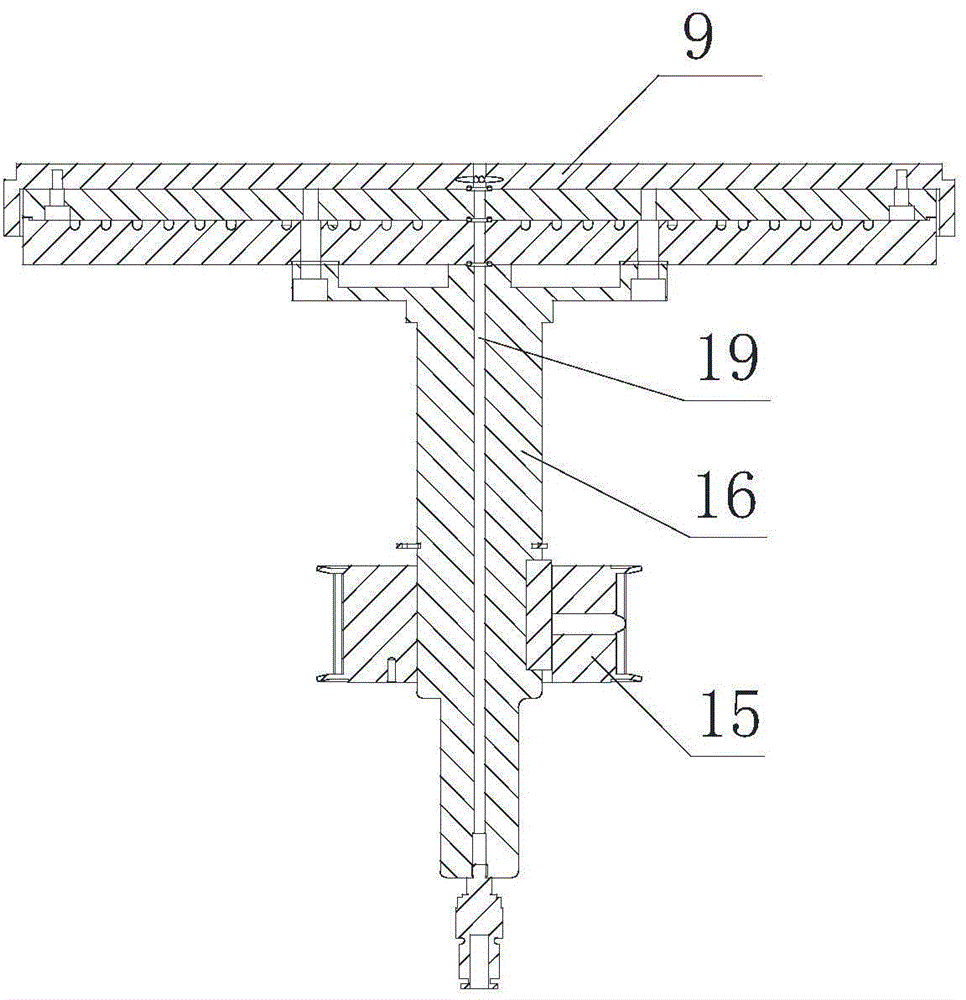
[0025] Such as Figure 1~2 As shown, the present invention includes an electric cylinder 1, a fixed plate 3, a scale 4, a spray head 6, a plastic cup assembly 7, a rotary adsorption mechanism 8 and a base plate 11, wherein the base plate 11 is fixed on the external equipment frame of the present invention, and the electric cylinder 1 is installed on the base plate 11 through a supporting frame 10, the electric cylinder 1 is provided with a moving beam 2, and the moving beam 2 is vertically arranged relative to the length direction of the supporting frame 10, and the moving beam 2 is A fixed plate 3 is provided, and a plurality of scales 4 are installed on the fixed plate 3 through the mounting frame 5 respectively, and a nozzle 6 is fixedly installed at the lower end of each scale 4, and all the nozzles 6 are driven by the electric cylinder 1 Translate synch...


PUM


Abstract

The invention relates to the field of semiconductor processing, in particular to a semiconductor made thick photoresist film coating device and an application method thereof. The semiconductor made thick photoresist film coating device comprises an electric cylinder, spraying heads, a photoresist cup assembly, a rotary adsorption mechanism and a base plate. The electric cylinder and the photoresist cup assembly are both arranged on the base plate. A movable beam is arranged on the electric cylinder. The spraying heads spraying heads of which the intervals and the height can be all adjusted are arranged on the movable beam. The rotary adsorption mechanism is provided with a rotary adsorption disk used for adsorbing a wafer. The adsorption disk is arranged in the middle of the photoresist cup assembly. During photoresist film coating, the spraying heads are driven by the movable beam of the electric cylinder to move horizontally above the adsorption disk. The to-be-processed wafer is put on the adsorption disk. The multiple spraying heads are driven by the electric cylinder to move synchronously and horizontally and spraying photoresist, and then the wafer is fixedly adsorbed by the adsorption disk. The multiple spraying heads are driven by the electric cylinder to move synchronously and horizontally and spray the atomized photoresist. According to the semiconductor made thick photoresist film coating device and the application method thereof, even spraying is ensured, the film thickness of the whole wafer is made to be uniform, and edge protrusions of the wafer is avoided completely.

Description

technical field [0001] The invention relates to the field of semiconductor processing, in particular to a thick glue film coating device made of semiconductors and a method for using the same. Background technique [0002] In the field of semiconductor processing, in the existing spraying photoresist technology, the coating of thick film is processed by spin coating. Because the film is thick, it needs to be coated more than two times and the spreading process is slow. It is very low, and the uniformity is difficult to control, and there is a circle of bumps on the edge of the wafer after spin coating, which makes the edge of the wafer unusable and reduces the utilization rate of the product. As semiconductor production refinement and high integration requirements are getting higher and higher, wafer productivity and yield are getting more and more attention. In various processing processes, the treatment of spraying photoresist on the wafer surface is particularly important...

Claims


Application Information

Patent Timeline
Patent Type & Authority Applications(China)
IPC IPC(8): B05C5/00B05C13/02H01L21/027B05B15/68
Inventor 王绍勇汪涛卢美丽
Owner SHENYANG KINGSEMI CO LTD
Why Eureka
Try Eureka