
Full-temperature-area thermoelectricity bi-field scanning electron microscope (SEM) in-situ physical property testing desk

A field scanning and measuring stage technology, applied in the field of micro-nano materials, can solve the problems of uneven temperature distribution of the sample stage, poor heat dissipation effect of the sample stage, and inability to expand multiple physical fields, so as to reduce thermal conductivity, reduce thermal contact, and quickly cooling effect

Inactive Publication Date: 2016-07-20
LANZHOU UNIVERSITY
View PDF6 Cites 8 Cited by
  • Summary
  • Abstract
  • Description
  • Claims
  • Application Information

AI Technical Summary

Problems solved by technology

[0008] The purpose of the present invention is to provide a thermoelectric two-field scanning electron microscope in-situ physical property measurement platform with a full temperature zone, aiming to solve the problem that the existing commercial or self-developed scanning electron microscope variable temperature sample platform has a small temperature zone and has limitations on material research; Inability to expand multi-physics fields, resulting in a single function, unable to realize material performance research under multi-field control, poor heat dissipation effect of the sample stage, temperature changes and sample drift caused by electron beam irradiation, and uneven temperature distribution of the sample stage

Method used


Image

  • Full-temperature-area thermoelectricity bi-field scanning electron microscope (SEM) in-situ physical property testing desk
  • Full-temperature-area thermoelectricity bi-field scanning electron microscope (SEM) in-situ physical property testing desk
  • Full-temperature-area thermoelectricity bi-field scanning electron microscope (SEM) in-situ physical property testing desk

Examples


Embodiment Construction

[0033] In order to make the object, technical solution and advantages of the present invention more clear, the present invention will be further described in detail below in conjunction with the examples. It should be understood that the specific embodiments described here are only used to explain the present invention, not to limit the present invention.

[0034] The application principle of the present invention will be described in detail below in conjunction with the accompanying drawings.

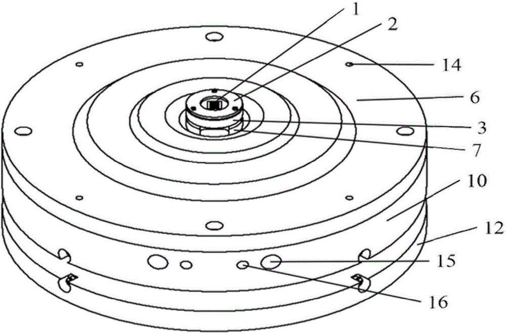
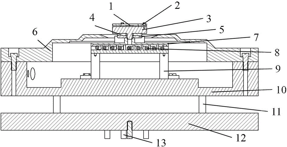
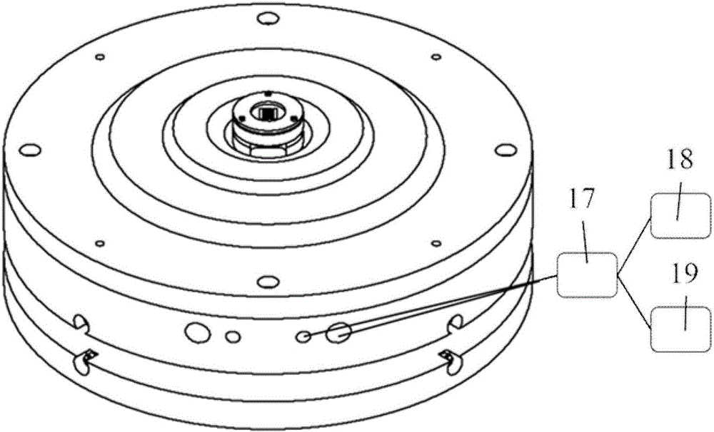
[0035] like Figure 1-Figure 3 As shown, the thermoelectric two-field scanning electron microscope in-situ physical property measurement platform of the embodiment of the present invention mainly includes: sample 1, sample pressing tablet 2, heat conduction platform 3, temperature measuring element 4, heating element 5, sample stage cover 6, Cooling table top 7, cooling pipe 8, cooling table bottom 9, heat insulation table top 10, heat insulation column 11, heat insulation table botto...


PUM


Abstract

The invention discloses a full-temperature-area thermoelectricity bi-field SEM in-situ physical property testing desk which comprises a sample, a sample pressing sheet, a heat conduction bench, a temperature measurement element, a heating element, a sample bench cover, a cooling bench top, a cooling pipe, a cooling bench bottom, a heat insulation bench top, a heat insulation pole, a heat insulation bench bottom, an SEM connecting pole, a function expansion aperture, a cooling pipe hole, a cable hole, a vacuum flange module, a cooling control module and a PID temperature control and electricity test module. Thermoelectric properties of sample materials can be researched, and research on in-situ performance under regulation and control of multiple physical fields of mechanics, electricity and calorifics can be realized, and rapid refrigeration cooling is achieved. Heat conduction effect is reduced by making full use of the structure of a sample bench, and discharging phenomenon and layered lines due to image heat interference in a heating process can be prevented. A coaxial annular heating module is employed, and red copper with excellent thermal conductivity is used for making a sample heat conduction bench. The temperature measurement element is arranged between the heating module and a sample, and accurate temperature measurement can be realized.

Description

technical field [0001] The invention belongs to the technical field of micro-nano materials, and in particular relates to an in-situ physical property measurement platform of a thermoelectric two-field scanning electron microscope in a full temperature zone. Background technique [0002] In situ technology in scanning electron microscopy is a rapidly developing research field. It can observe and study the structural changes and physical properties of materials and devices in real time under microscopic conditions, which is conducive to accurately understanding the actual use effect of materials and devices. Thermoelectricity and phase transition are important properties of materials and devices, which can reflect many physical properties of materials and devices. Thermoelectric materials with thermoelectric properties can realize the mutual conversion of heat energy and electric energy without mechanical parts, no noise, and realize thermoelectric power generation or thermoe...

Claims


Application Information

Patent Timeline
IPC IPC(8): H01J37/20H01J37/28
CPCH01J37/20H01J37/28H01J2237/20H01J2237/28
Inventor 彭勇郑修军黄源清夏卫星张军伟马鸿斌关超帅胡阳杨保林薛德胜
Owner LANZHOU UNIVERSITY
Learn More