Plasma processing device and method for adjusting plasma distribution

A plasma and processing device technology, which is applied in the field of semiconductor processing equipment, can solve problems such as inconsistent device feature size, unsatisfactory plasma density uniformity, semiconductor device process control and yield impact, and achieve uniform processing rate.

Active Publication Date: 2017-11-10
ADVANCED MICRO FAB EQUIP INC CHINA
View PDF7 Cites 0 Cited by
  • Summary
  • Abstract
  • Description
  • Claims
  • Application Information

AI Technical Summary

Problems solved by technology

[0003] However, in practical applications, the uniformity of the plasma density generated by using the above-mentioned plasma device is not ideal, and the density of the generated plasma has a characteristic distribution in which the edge region is higher than the middle region
However, because the rate of plasma treatment of the substrate is related to the plasma density distribution or the distribution of atomic groups, it will eventually cause uneven plasma treatment processes: for example, the edge of the substrate is etched or the processing rate is fast, and the middle area is etched or processed. slow processing
This will easily cause inconsistency in the feature size of the device within the entire substrate range, which has a great impact on the process control and yield of semiconductor device manufacturing.

Method used


Image

  • Plasma processing device and method for adjusting plasma distribution
  • Plasma processing device and method for adjusting plasma distribution
  • Plasma processing device and method for adjusting plasma distribution

Examples


Embodiment Construction

[0023] In order to make the content of the present invention clearer and easier to understand, the content of the present invention will be further described below in conjunction with the accompanying drawings. Of course, the present invention is not limited to this specific embodiment, and general replacements known to those skilled in the art are also covered within the protection scope of the present invention.

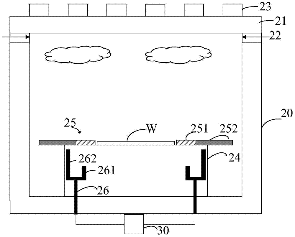
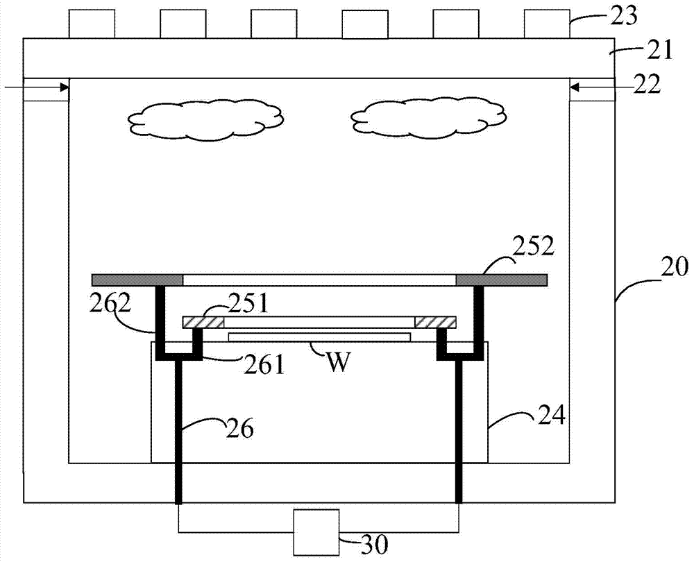
[0024] Figure 2a with Figure 2b is a schematic structural view of a plasma processing apparatus according to an embodiment of the present invention. It should be understood that the plasma processing device in the present invention can be a device such as plasma etching, plasma physical vapor deposition, plasma chemical vapor deposition, plasma surface cleaning, etc., and the plasma processing device is only exemplary. Fewer or more constituent elements may be included, or the arrangement of the constituent elements may be the same as or different from that sho...


PUM


Abstract

The invention discloses a plasma processing device. The plasma processing device comprises a reaction cavity chamber and a driving unit, wherein the reaction cavity chamber comprises a base, a combined shielding ring and a plurality of fork-shaped connection rods, the base is used for carrying a substrate to be processed, the combined shielding ring is arranged around the periphery of the substrate and comprises an inner ring and an outer ring, the upper end of each fork-shaped connection rod is divided into an inner strut and an outer strut, the outer strut is in correspondence to the outer ring, the inner strut is in correspondence to the inner ring, a support part is arranged at the top end of each strut, the height of the support part at the outer strut is higher than the height of the support part at the inner strut, and the driving unit drives the fork-shaped connection rods to vertically move between a first position and a second position; when the fork-shaped connection rods are arranged at the first position, the support parts of the two strut are not in contact with the combined shielding ring; and when the fork-shaped connection rods are risen to the second position, the outer ring props against the support part of the outer strut, and the inner ring props against the support part of the inner strut. By the plasma processing device, the plasma distribution uniformity on the substrate surface can be improved.

Description

technical field [0001] The invention relates to semiconductor processing equipment and methods, in particular to a plasma processing device and a method for adjusting plasma distribution using the processing device. Background technique [0002] Plasma processing devices are widely used in various semiconductor manufacturing processes, such as deposition processes (such as chemical vapor deposition), etching processes (such as dry etching), and the like. Taking the plasma etching process as an example, figure 1 A schematic structural diagram of an inductively coupled plasma etching device in the prior art is shown. The top of the reaction chamber 10 has an insulating cover plate 11, the bottom of the reaction chamber 10 is provided with an electrostatic chuck 14 for clamping the substrate W to be processed, and the air inlet unit 12 is arranged under the insulating cover plate 11 on the side wall of the reaction chamber 10. . An inductive coupling coil 13 is arranged on t...

Claims


Application Information

Patent Timeline
Patent Type & Authority Patents(China)
IPC IPC(8): H01J37/32
Inventor 李俊良
Owner ADVANCED MICRO FAB EQUIP INC CHINA
Why Eureka
Try Eureka