

Semiconductor and fabrication method thereof
A technology for semiconductors and devices, applied in the field of semiconductor devices and their preparation, can solve the problems that the source and drain regions need to be sufficiently large and small.
Active Publication Date: 2016-07-20
SEMICON MFG INT (SHANGHAI) CORP
View PDF5 Cites 2 Cited by
- Summary
- Abstract
- Description
- Claims
- Application Information
AI Technical Summary
Problems solved by technology
The source region, drain region and gate structure all need to be connected to the upper conductive layer through contact holes, so in the general device manufacturing process, usually after the source region, drain region and gate structure of the device are formed, The communication between it and other interconnection layers is realized through the contact holes connected to these three regions respectively, which makes the source region and drain region of the device need to be large enough to meet the complete contact with the bottom of the contact hole, This virtually inhibits the further reduction of the device size and becomes a bottleneck in the actual manufacturing process of semiconductor devices.
Method used
View moreImage
Smart ImageViewing Examples

Examples
preparation example Construction
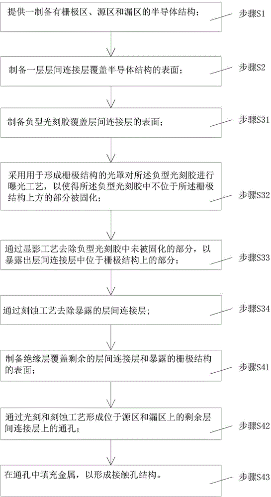
[0049] The preparation method of interlayer connecting layer of the present invention mainly comprises the following steps:
[0050] Step S1, providing a semiconductor structure prepared with a gate structure, a source region and a drain region;
[0051] Step S2, preparing a layer of interlayer connection layer covering the surface of the semiconductor structure;
[0052] Step S3, removing the interlayer connection layer covering the gate structure;
[0053] Step S4 , continuing to prepare a contact hole structure on the remaining interlayer connection layer located on the source region and the drain region.
Login to View More PUM
 Abstract
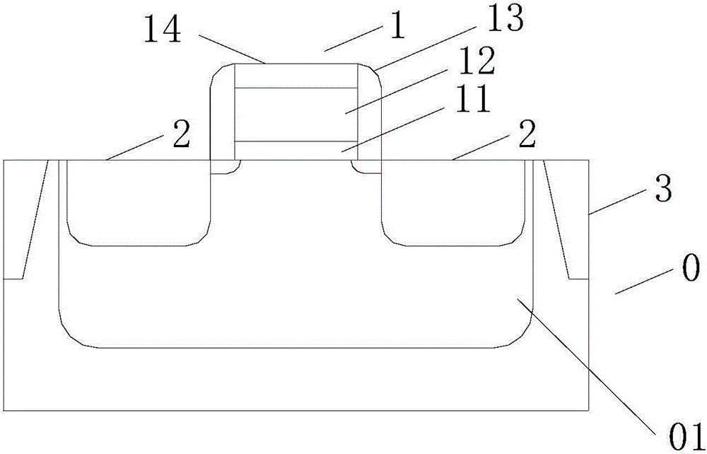
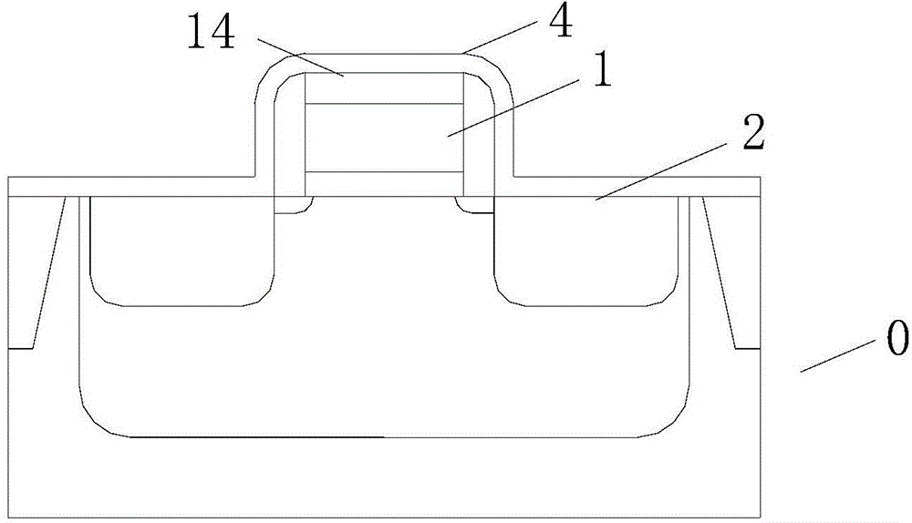
The invention provides a semiconductor device and a fabrication method thereof. By arranging a poly-silicon inter-layer connection layer on the surfaces of a source region and a drain region of the device, the source region and the drain region of the device can extend to the surface of a substrate by the inter-layer connection layer, are connected with contact holes by the inter-layer connection layer and are connected other inter-connection layers at the upper part, so that the areas of source-drain regions are not needed to be excessive large due to catering to the contact holes, and the probability is provided for further reducing the areas of the source region and the drain region. Further, the poly-silicon inter-layer connection layer in the semiconductor device only covers the surface of an active region and are not arranged on the side wall of a grid or other regions, thus, parasitic capacitance between the source-drain regions and the grid cannot be generated, and meanwhile, the device is enabled to have required breakdown voltage.
Description
technical field [0001] The invention relates to the field of semiconductor device manufacturing, in particular to a semiconductor device and a preparation method thereof. Background technique [0002] Since various products integrated with semiconductor devices need to become lighter and smaller, this requires semiconductor devices to develop towards smaller process sizes and more extreme process requirements. [0003] For a MOS device, it generally has a source region, a drain region and a gate structure. The source region, drain region and gate structure all need to be connected to the upper conductive layer through contact holes, so in the general device manufacturing process, usually after the source region, drain region and gate structure of the device are formed, The communication between it and other interconnection layers is realized through the contact holes connected to these three regions respectively, which makes the source region and drain region of the device ...
Claims
Login to View More Application Information
Patent Timeline
 Patent Type & AuthorityApplications(China)
IPC IPC(8): H01L21/768H01L21/336H01L23/538H01L29/78
Inventor王鷁奇蔡建祥
OwnerSEMICON MFG INT (SHANGHAI) CORP