Insulated gate bipolar transistor structure

A bipolar transistor, insulated gate technology, applied in semiconductor devices, electrical components, circuits, etc., can solve problems such as reduction, and achieve the effect of low on-state voltage drop

Active Publication Date: 2016-07-20
宁波安建半导体有限公司
View PDF4 Cites 3 Cited by
  • Summary
  • Abstract
  • Description
  • Claims
  • Application Information

AI Technical Summary

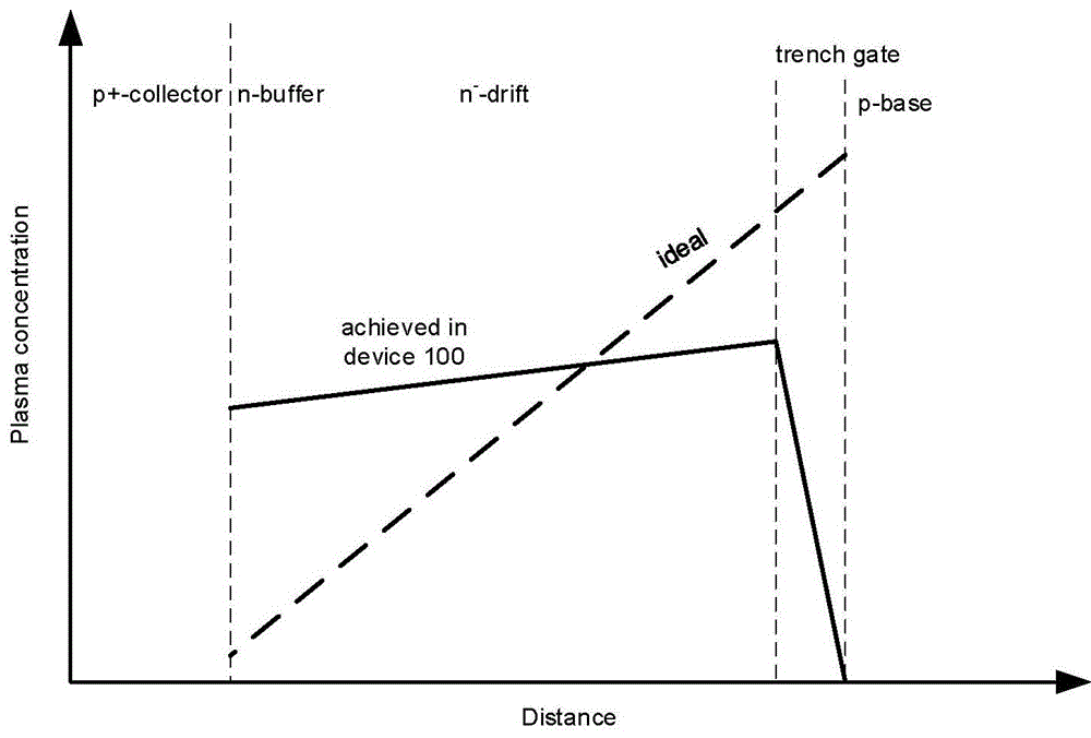
Problems solved by technology

This reduced concentration makes the on-state voltage drop of device 100 relatively larger than p-i-n diode

Method used


Image

  • Insulated gate bipolar transistor structure
  • Insulated gate bipolar transistor structure
  • Insulated gate bipolar transistor structure

Examples


Embodiment Construction

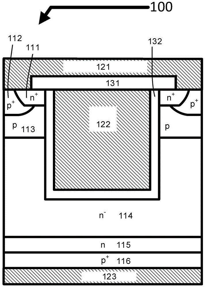
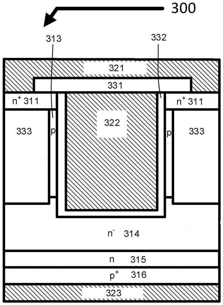
[0022] This embodiment is a preferred implementation mode of the present invention, and other principles and basic structures that are the same or similar to this embodiment are within the protection scope of the present invention.

[0023] The present invention will be described using n-channel devices, but it will be understood in the following description that the present invention is also applicable to p-channel devices, and the structure of p-channel devices is similar to that of n-channel devices, except that the doped regions The miscellaneous type is just the opposite, which is recognized in the industry, so the present invention only uses the N-channel as an example to illustrate the structure, and omits the structure description for the p-channel device.

[0024] In the description of the present invention, the heavily doped n-type region is denoted n + , and the heavily doped p-type region is labeled p + . In silicon, heavily doped regions typically have 1×10 19 ...


PUM


Abstract

The invention discloses an insulated gate bipolar transistor structure. The insulated gate bipolar transistor structure includes a collector located at the bottom of the insulated gate bipolar transistor structure, a collection region of a second conductivity type arranged on the top of the collector, a buffer region of a first conductivity type which is arranged at the top of the collection region, a drift region of the first conductivity type which is arranged at the top of the buffer region, a buried dielectric which is partially enclosed by the upper surface of the drift region and is made of an insulation material, an ultra-thin polysilicon base region of the second conductivity type which is arranged at the top of the drift region and is adjacent to the buried dielectric, a gate dielectric which is partially enclosed by the upper surface of the drift region and is adjacent to the polysilicon base region, a gate electrode which is partially enclosed by the gate dielectric, a polysilicon emission region of the first conductivity type which is adjacent to the gate dielectric and is located at the tops of the base region and the buried dielectric, a polysilicon diffusion region of the second conductivity type which is parallel to the emission region, an emitter which is in short connection with the emission region and the diffusion region, and an interlayer dielectric which isolates the emitter from the gate electrode. The insulated gate bipolar transistor structure has theoretical minimum on-state voltage drop.

Description

technical field [0001] The invention discloses a power semiconductor device, in particular an insulated gate bipolar transistor structure. Background technique [0002] Insulated-gate bipolar transistors (IGBTs) have been widely used in high-voltage power electronic systems, such as variable-frequency drives and inverters. An ideal device should have low power loss. The conduction loss of IGBT is the main component of power loss, and the conduction loss can be characterized by the on-state voltage of the device. [0003] Please refer to the attached picture, figure 1 A cross section of a prior art IGBT device 100 is shown in . Device 100 is a PNP bipolar junction transistor controlled by MOS, and the MOS channel is controlled by n + Emitter region 111, p base region 113, n - The drift region 114, the gate dielectric 132 and the gate electrode 122 are composed, and the on-state and off-state of the device are controlled by the MOS channel. In the on-state of the device 10...

Claims


Application Information

Patent Timeline
Patent Type & Authority Applications(China)
IPC IPC(8): H01L29/739H01L29/06H01L29/10
CPCH01L29/0657H01L29/10H01L29/7395
Inventor 周贤达舒小平徐远梅
Owner 宁波安建半导体有限公司
Why Eureka
Try Eureka