Ion implantation method of substrate back of power device

A technology of power devices and ion implantation, which is applied in the direction of semiconductor devices, semiconductor/solid-state device manufacturing, electrical components, etc., can solve the problems that power devices cannot be used, power device leakage current, on-state voltage drop switching time becomes larger, etc., to achieve Reduced on-state voltage drop, reduced switching time, and reduced contact resistance

Inactive Publication Date: 2012-06-27
UNIV OF ELECTRONICS SCI & TECH OF CHINA +1
View PDF0 Cites 2 Cited by
  • Summary
  • Abstract
  • Description
  • Claims
  • Application Information

AI Technical Summary

Problems solved by technology

The mainstream manufacturing process of the above-mentioned various power devices is to directly manufacture metal electrodes after impurity ion implantation and annealing. However, after impurity implantation on the back of the silicon wafer, an impurity distribution layer with a certain depth will be formed after annealing activation. The impurity layer will cause the back metal and the implanted impurity region to fail to form a good ohmic contact, bring unnecessary parasitic multi-layer structure, increase the leakage current, on-state voltage drop and switching time of the power device, and directly lead to the developed Power devices cannot be used

Method used


Image

  • Ion implantation method of substrate back of power device
  • Ion implantation method of substrate back of power device
  • Ion implantation method of substrate back of power device

Examples


Embodiment Construction

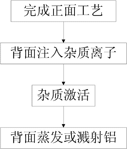
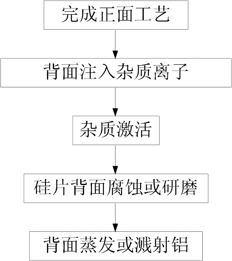
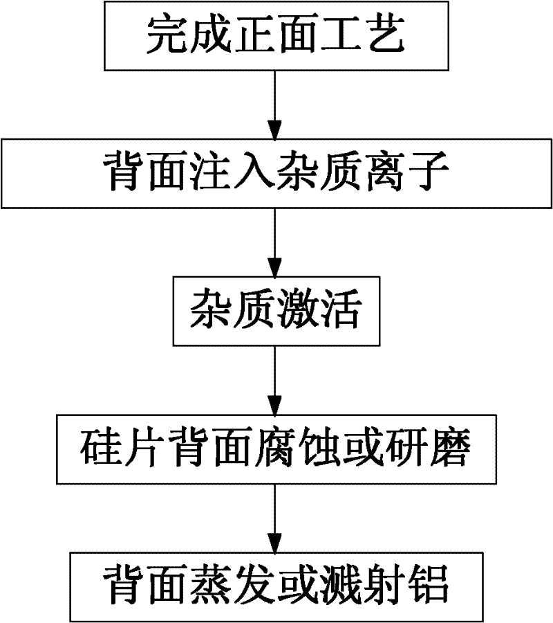
[0023] A method of ion implantation on the backside of a power device substrate, such as figure 2 As shown, after completing the front-side process steps of the power device, an operation including the following steps is performed:

[0024] Step 1: Implanting boron or phosphorus impurity ions on the back of the power device substrate;

[0025] Step 2: Activation of impurity ions;

[0026] Step 3: The back side of the power device substrate is thinned to the impurity injection layer;

[0027] Step 4: growing a metal aluminum layer on the back of the power device substrate by sputtering or evaporation.

[0028] In the above scheme, when implanting boron or phosphorus impurity ions on the back of the power device substrate in step 1, the implantation dose of the impurity ions is 1×10 13 ~2×10 15 cm -2 , the energy range is 30Kev~300Kev, and the injection depth is The present invention adopts a larger implantation energy than the usual ion implantation process, so that the...


PUM


Abstract

The invention relates to an ion implantation method of a substrate back of a power device, belonging to the technical field of semiconductor power devices. The ion implantation method disclosed by the invention comprises the following steps of: after finishing steps of a front face process of the power device, thinning the substrate back to an impurity implantation layer and then depositing a metal aluminum layer by utilizing a corrosion or grinding method after ion implantation (thinning or non-thinning process can be carried out on the substrate back before the ion implantation) and ion activation are finished, but not directly carrying out metal aluminum layer deposition like the traditional process. Therefore, the contact resistance between the subsequently deposited metal aluminum and the substrate can be reduced, unnecessary parasitic multi-layer structures can be eliminated, the leakage current and the on-state voltage drop of the power device are reduced, and the switching time of the power device is shortened. The ion implantation method of the substrate back of the power device, disclosed by the invention, is suitable for semiconductor power devices made from semiconductor materials, such as bulk-silicon, silicon carbide, gallium arsenide, indium phosphide or germanium silicon and the like.

Description

technical field [0001] The invention belongs to the technical field of semiconductor power devices and relates to the manufacturing technology of semiconductor power devices. Background technique [0002] Power semiconductor technology is the core of power electronics technology. With the development of microelectronics technology, modern power semiconductor technology represented by gate-controlled power devices and intelligent power integrated circuits has developed rapidly since the 1980s, which has greatly promoted Advances in power electronics. The continuous progress of power electronics technology in turn promotes the development of power semiconductor technology in the direction of high frequency, high temperature, high voltage, high power, intelligence and systematization. After more than 40 years of development, power semiconductor devices have continued to improve in device manufacturing technology. They have experienced discrete devices represented by thyristors...

Claims


Application Information

Patent Timeline
Patent Type & Authority Patents(China)
IPC IPC(8): H01L21/28H01L21/02H01L21/265
Inventor 李泽宏肖璇张超吴宽谢加雄李婷刘小龙
Owner UNIV OF ELECTRONICS SCI & TECH OF CHINA
Why Eureka
Try Eureka