Transverse diffusion field effect transistor and manufacturing method therefor

A technology for field effect transistors and manufacturing methods, applied in semiconductor/solid-state device manufacturing, semiconductor devices, electrical components, etc., to achieve the effects of reducing the JFET effect, increasing the current conduction area, and reducing the on-resistance

Active Publication Date: 2016-07-20
SHANGHAI HUAHONG GRACE SEMICON MFG CORP
View PDF3 Cites 11 Cited by
  • Summary
  • Abstract
  • Description
  • Claims
  • Application Information

AI Technical Summary

Problems solved by technology

[0015] like Figure 2B shown, is figure 1 The depletion region simulation diagram of the existing device shown; it can be seen that the drift region in the region corresponding to the dotted circle 203 has not been fully depleted

Method used


Image

  • Transverse diffusion field effect transistor and manufacturing method therefor
  • Transverse diffusion field effect transistor and manufacturing method therefor
  • Transverse diffusion field effect transistor and manufacturing method therefor

Examples


Embodiment Construction

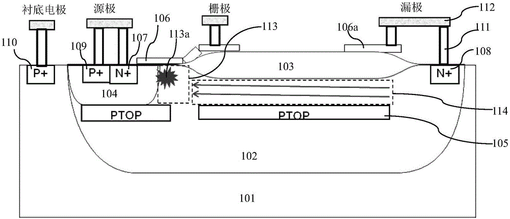
[0072] like Figure 4 As shown, it is a schematic structural diagram of a lateral diffusion field effect transistor according to an embodiment of the present invention; taking an N-type device as an example, a lateral diffusion field effect transistor according to an embodiment of the present invention includes:

[0073] An N-type doped drift region 2 is formed in a P-type semiconductor substrate such as a silicon substrate 1; in Embodiment 1 of the present invention, the drift region 2 is directly composed of an N-type epitaxial layer 2, and the N-type epitaxial layer 2 is formed on the surface of the semiconductor substrate 1.

[0074] The P-type doped channel region 4 is formed in the drift region 2 of the semiconductor substrate 1 .

[0075] A P-type doped buried layer, namely PTOP, is formed in the drift region 2, and the buried layer is divided into multiple buried layer segments with different concentrations and different depths, Figure 4 The buried layer segment 5a ...


PUM


Abstract

The invention discloses a transverse diffusion field effect transistor. The transverse diffusion field effect transistor comprises a second-conductive-type-doped buried layer formed in a first-conductive-type-doped drifting region; the buried layer is provided with multiple buried layer sections with different concentrations and different depths; each adjacent two buried layer sections are arranged in a staggered manner longitudinally, so that a JFET effect between a channel region and the drifting region is lowered, and the current conduction region in the drifting region is enlarged when the device is conducted; the doping concentration of the buried layer section nearest to the channel region is greater than that of other buried layer sections; and due to the doping concentration of the buried layer section nearest to the channel region, the auxiliary drifting region on the side face of the channel region can be fully depleted at the initial stage of a drain terminal voltage. The invention also discloses a manufacturing method for the transverse diffusion field effect transistor. By adoption of the transverse diffusion field effect transistor, the low voltage breakdown can be prevented, the breakdown voltage can be increased, the conduction region of the leakage current can be enlarged, and the conduction resistance of the device can be lowered.

Description

technical field [0001] The invention relates to the field of semiconductor integrated circuit manufacturing, in particular to a lateral diffusion field effect transistor; the invention also relates to a manufacturing method of the lateral diffusion field effect transistor. Background technique [0002] Ultra-high voltage lateral diffusion field effect transistor (LDMOS) usually inserts a buried layer opposite to the conductivity type of the drift region in the drift region. The buried layer can help the drift region to be depleted, so that the concentration of the drift region can be appropriately increased, and the ultra-high voltage LDMOS can also be guaranteed. breakdown voltage. [0003] like figure 1 Shown is a schematic diagram of the structure of the existing lateral diffusion field effect transistor; taking N-type LDMOS as an example, the existing LDMOS includes: [0004] The drift region 102 is composed of a deep N well formed in a P-type semiconductor substrate s...

Claims


Application Information

Patent Timeline
Patent Type & Authority Applications(China)
IPC IPC(8): H01L29/78H01L21/336
CPCH01L29/66681H01L29/7816H01L29/0634H01L29/404H01L29/42368
Inventor 钱文生
Owner SHANGHAI HUAHONG GRACE SEMICON MFG CORP
Why Eureka
Try Eureka