Semiconductor on insulator (SOI) lateral metal-oxide-semiconductor field-effect-transistor (MOSFET) device and integrated circuit

A technology of integrated circuits and devices, which is applied in the field of SOI lateral MOSFET devices and integrated circuits, can solve problems such as poor process repeatability and sensitivity, and achieve the effects of reducing process costs, increasing withstand voltage, and improving withstand voltage

Inactive Publication Date: 2013-01-30
UNIV OF ELECTRONICS SCI & TECH OF CHINA
View PDF0 Cites 0 Cited by
  • Summary
  • Abstract
  • Description
  • Claims
  • Application Information

AI Technical Summary

Problems solved by technology

Due to the particularity of SOI, its optimization rules will be different, and in the conventional planar gate structure, due to the interaction of the semiconductor buried layer, the gate field plate and the PN junction (the junction of the body region and the drift region), the device The withstand voltage is very sensitive to the position of the semiconductor buried layer, and the process repeatability is very poor (such as Figure 8 shown)

Method used


Image

  • Semiconductor on insulator (SOI) lateral metal-oxide-semiconductor field-effect-transistor (MOSFET) device and integrated circuit
  • Semiconductor on insulator (SOI) lateral metal-oxide-semiconductor field-effect-transistor (MOSFET) device and integrated circuit
  • Semiconductor on insulator (SOI) lateral metal-oxide-semiconductor field-effect-transistor (MOSFET) device and integrated circuit

Examples


Embodiment 1

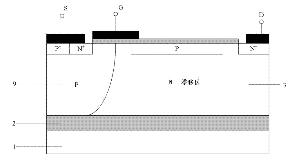
[0055] Fig. 4(a) is a cross-sectional view showing the cell structure of the N-channel double-gate SOI lateral MOSFET device in which the P-type semiconductor buried layer 4 and the body region 9 are in contact with each other according to the present invention. As shown in Figure 4(a), in an SOI lateral MOSFET device, a substrate layer 1, a dielectric buried layer 2, and an active layer 3 are sequentially stacked from bottom to top, and the active layer 3 has surfaces respectively located on the active layer 3 And the body region 9 and the drain region 12 separated from each other, and the planar gate channel region 14 ′, source region 11a, body contact region 10 and The source region 11b, the active layer 3 located between the body region 9 and the drain region 12 is a drift region, its conductivity type is opposite to that of the body region 9, and the active layer 3 is provided with a semiconductor buried layer 4 below its surface, The semiconductor buried layer 4 and the ...

Embodiment 2

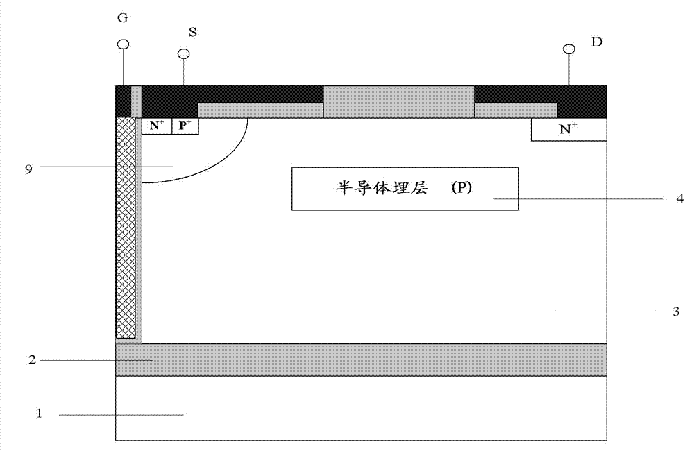
[0058] Figure 5 It is a cross-sectional view showing the cell structure of the P-channel double-gate SOI lateral MOSFET device with the N-type semiconductor buried layer 4 of the present invention. Such as Figure 5 As shown, the only difference between it and FIG. 4(a) is that the active layer 3, semiconductor buried layer 4, source regions 11a, 11b, drain region 12, body region 9 and body contact region 10 of the device in this example are The conductivity type of the material is opposite to that of the corresponding region of the N-channel double-gate SOI lateral MOSFET device, and the same technical effect as that of Embodiment 1 can also be obtained. That is to say, the double-gate MOS controlled lateral SOI device with semiconductor buried layer of the present invention can be used to manufacture both N-channel devices and P-channel devices.

Embodiment 3

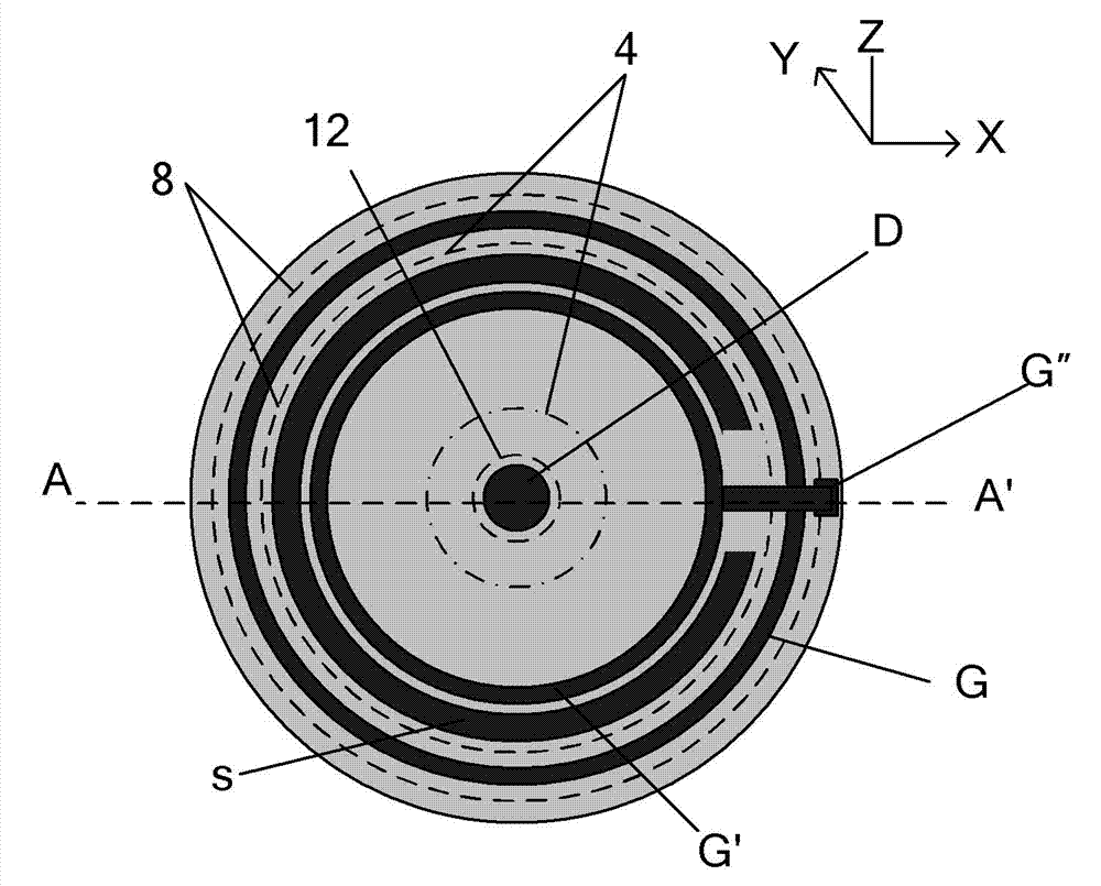
[0060]In this embodiment 3, the top view of the device is a symmetrical structure, the drain region 12 is located at the center of the device, and from the drain region 12 to the outside are the semiconductor buried layer 4, the body region 9, the source region 11a, the body contact region 10, and the source region 11b and the trench gate structure 8, the trench gate structure 8 is located at the periphery of the device. Below, according to Figure 6 and Figure 7 , the present embodiment 3 will be described.

[0061] Figure 6 It is a schematic diagram showing the cell layout of an SOI lateral MOSFET device with an axisymmetric structure of the present invention, that is, the xz plane view, wherein AA' is along the x direction, and the vertical direction perpendicular to the paper is the y direction. Should Figure 6 Take the circular figure as an example to describe the axisymmetric structure. The drain electrode D is located at the center of the device. The device tak...


PUM


Abstract

A silicon-on-insulator (SOI) lateral MOSFET device and the integrated circuit thereof are provided. In said device, an active layer (3) includes a body region (9) and a drain region (12) which are located on the surface of the active layer (3) respectively and are separated from each other, and also a planar gate channel region (14'), a source region (11a), a body contact region (10) and a source region (11b) which are located on the surface of the body region (9) and are set in sequence from the side adjacent to the drain region (12). The active layer (3) located between the body region (9) and the drain region (12) is a drift region, wherein the drift region and the body region (9) have opposite conduction types. A semiconductor buried layer (4) is set beneath the surface of the active layer (3), wherein the semiconductor buried layer (4) and the body region (9) have the same conduction type. Said device has a trench gate structure (8) and a planar gate structure (8'), wherein the trench gate structure (8) contacts with the body region (9) and longitudinally extends from the surface of the active layer (3) to a dielectric buried layer (2), and the planar gate structure (8') is formed above the body region (9). Said device has the advantages of high withstand voltage, low specific on-resistance, low power consumption, low cost, and easy miniaturization and integration.

Description

technical field [0001] The present invention relates to semiconductor power devices and integrated circuits, in particular to a SOI (Semiconductor On Insulator, semiconductor on insulating substrate) lateral MOSFET (Metal-Oxide-Semiconductor Field-Effect- Transistor, Metal-Oxide-Semiconductor Field-Effect Transistor) devices and integrated circuits with them. Background technique [0002] SOI is to introduce a dielectric buried layer between the top semiconductor (called the active layer) and the substrate layer (which can be a semiconductor or insulating medium), and make semiconductor devices or circuits in the active layer. In integrated circuits, high-voltage devices and low-voltage circuits are usually isolated by isolation grooves 30, and between the active layer 3 and the substrate layer 1 are isolated by a dielectric buried layer 2 (such as figure 1 shown). Therefore, compared with bulk silicon technology, SOI technology has the advantages of small parasitic effect...

Claims


Application Information

Patent Timeline
Patent Type & Authority Patents(China)
IPC IPC(8): H01L29/78H01L29/423H01L27/085
CPCH01L29/4236H01L29/1095H01L29/7825H01L29/0634H01L29/0696H01L29/7824H01L29/4238H01L27/0922H01L29/7831
Inventor 罗小蓉姚国亮雷天飞王元刚张波李肇基
Owner UNIV OF ELECTRONICS SCI & TECH OF CHINA
Why Eureka
Try Eureka