LED chip modularized packaging method

A technology of LED chip and packaging method, applied in the field of microelectronics, can solve the problems of difficult to guarantee the lamp surface, poor reliability, short life, etc., and achieve the effect of solving the problem of weak wire bonding, improved connection efficiency and high price.

Active Publication Date: 2016-07-20
SHANGHAI INTEGRATED CIRCUIT RES & DEV CENT
View PDF3 Cites 1 Cited by
  • Summary
  • Abstract
  • Description
  • Claims
  • Application Information

AI Technical Summary

Problems solved by technology

However, in terms of technology, COB packaging still has shortcomings such as light decay, short life, and poor reliability. This is because COB products are sealed first. When the lamp surface is processed by reflow soldering, the high temperature of 240 degrees in the furnace will not cause damage to the lamp

Method used


Image

  • LED chip modularized packaging method
  • LED chip modularized packaging method
  • LED chip modularized packaging method

Examples


Embodiment Construction

[0027] In order to make the content of the present invention clearer and easier to understand, the content of the present invention will be further described below in conjunction with the accompanying drawings. Of course, the present invention is not limited to this specific embodiment, and general replacements known to those skilled in the art are also covered within the protection scope of the present invention.

[0028] The following is attached Figure 1-11 The present invention will be described in further detail with specific examples. It should be noted that the drawings are all in a very simplified form, using imprecise scales, and are only used to facilitate and clearly achieve the purpose of assisting in describing the present embodiment.

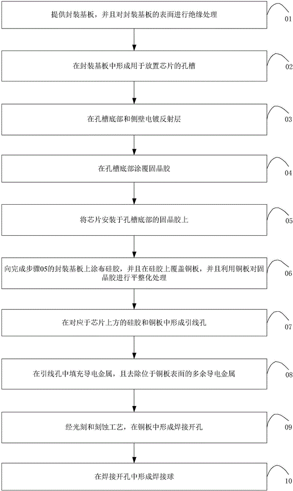
[0029] see figure 1 , the modular packaging method of the LED chip of this embodiment includes:

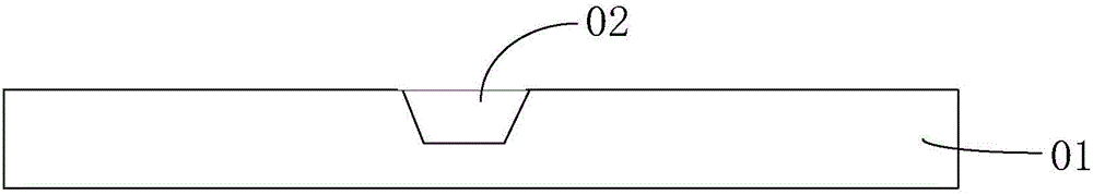
[0030] Step 01: providing a packaging substrate, and insulating the surface of the packaging substrate;

[0031] Specifically, s...


PUM


Abstract

The invention provides an LED chip modularized packaging method comprising the steps that a packaging substrate is provided, and insulation processing is performed on the surface of the packaging substrate; a hole groove used for placing a chip is formed in the packaging substrate; a reflecting layer is electroplated on the bottom part and the side walls of the hole groove; solid crystal glue is coated on the bottom part of the hole groove; the chip is installed on solid crystal glue of the bottom part of the hole groove; silica gel is coated on the packaging substrate and a copper plate covers silica gel, and the copper plate is flattened; a lead hole is formed in the corresponding silica gel and the copper plate above the chip; conductive metal is filled in the lead hole and residual conductive metal on the surface of the copper plate is removed; welding holes are formed in the copper plate through the photolithography and etching technology; and welding balls are formed in the welding holes. Damage of high temperature of the conventional reflow welding technology to the chip can be avoided, the problem that lead bonding is not firm due to the welding technology can be solved and cost can be reduced, and thus the method is suitable for large-scale production.

Description

technical field [0001] The invention relates to the technical field of microelectronics, in particular to a modular packaging method for LED chips. Background technique [0002] Packaging process technology plays a vital role in LED performance. The selection of LED packaging method, material, structure and process is mainly determined by factors such as chip structure, photoelectric / mechanical characteristics, specific application and cost. With the increase of power, especially the demand for the development of solid-state lighting technology, new and higher requirements are put forward for the optical, thermal, electrical and mechanical structures of LED packages. Traditional LED packaging uses gold wires to lead out the electrodes of the LED light-emitting chip, and at the same time uses a variety of materials to protect the light-emitting chip and gold wires, and at the same time completes the process of outputting electrical signals, protecting the normal operation of...

Claims


Application Information

Patent Timeline
Patent Type & Authority Applications(China)
IPC IPC(8): H01L33/00H01L33/52H01L33/62
CPCH01L33/005H01L33/52H01L33/62H01L2224/73267H01L2224/92244H01L2924/15153H01L2224/19H01L2224/32225H01L2224/32245H01L2224/18
Inventor 彭娟胡少坚陈寿面
Owner SHANGHAI INTEGRATED CIRCUIT RES & DEV CENT
Why Eureka
Try Eureka