High modulation speed light emitting diode, modulation method and manufacturing method thereof

A kind of technology of light emitting diode, modulation method

Active Publication Date: 2018-06-08
郴州隆合半导体有限公司
View PDF3 Cites 0 Cited by
  • Summary
  • Abstract
  • Description
  • Claims
  • Application Information

AI Technical Summary

Problems solved by technology

[0010] The purpose of the present invention is to provide a light-emitting diode with high modulation speed and its modulation method and manufacturing method, aiming at solving the problem that the existing light-emitting diode cannot meet the requirements of optical communication for modulation speed

Method used


Image

  • High modulation speed light emitting diode, modulation method and manufacturing method thereof
  • High modulation speed light emitting diode, modulation method and manufacturing method thereof
  • High modulation speed light emitting diode, modulation method and manufacturing method thereof

Examples


Embodiment Construction

[0027] The following will clearly and completely describe the technical solutions in the embodiments of the present invention with reference to the accompanying drawings in the embodiments of the present invention. Obviously, the described embodiments are only some, not all, embodiments of the present invention. Based on the embodiments of the present invention, all other embodiments obtained by persons of ordinary skill in the art without making creative efforts belong to the protection scope of the present invention.

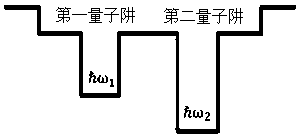
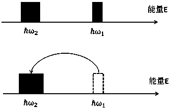
[0028] Such as figure 1 , the embodiment of the present invention provides a light-emitting diode with high modulation speed, the PN junction of the light-emitting diode has a junction region, the junction region is a region of voltage drop in the light-emitting diode, and the junction region includes a double quantum well structure, The double quantum well structure includes a first quantum well and a second quantum well, the bandgap of the first quantum well...


PUM


Abstract

The invention provides a high-modulation-speed light emitting diode, a modulation method thereof and a manufacturing method thereof. The PN junction region of the light emitting diode comprise a double-quantum-well structure. The double-quantum-well structure comprises a first quantum well and a second quantum well. The band gap of the first quantum well is larger than that of the second quantum well. The first quantum well radiates signal light, and the second quantum well radiates auxiliary light. Through a quantum tunneling effect, the first quantum well is coupled with the second quantum well. Through a dynamic process of carries in an energy space, the high-modulation-speed light emitting diode performs functions of realizing ultra-quick injection and ultra-quick extraction of the carriers from an energy area which is radiated by the signal light, reducing time required in rising edge and falling edge of the optical signal of the light emitting diode, and furthermore improving modulation speed of the light emitting diode.

Description

technical field [0001] The present invention relates to a light emitting diode and its modulation method and manufacturing method, in particular to a high modulation speed light emitting diode and its modulation method and manufacturing method. Background technique [0002] Light-emitting diode (LED) is a PN junction semiconductor optoelectronic device. The semiconductor materials used are generally binary or multi-component compound semiconductors of III-V and II-VI elements. Its radiation spectrum is determined by the band gap of the PN junction compound semiconductor material, covering from ultraviolet, visible to infrared bands. [0003] LED is a kind of spontaneous emission photoelectric device. Its light-emitting mechanism is that electrons are injected into the N region, holes are injected into the P region, and electrons and holes recombine spontaneously in the active region to emit photons. [0004] The electrons and holes in the PN junction are collectively refer...

Claims


Application Information

Patent Timeline
Patent Type & Authority Patents(China)
IPC IPC(8): H01L33/06H01L33/00
CPCH01L33/005H01L33/06
Inventor 王文峰项明明张家伟熊晖张军
Owner 郴州隆合半导体有限公司
Why Eureka
Try Eureka