Wave-absorbing metamaterial, antenna cover and antenna system
An antenna system and metamaterial technology, applied in the field of electromagnetic wave absorbing materials, can solve the problems of serious reflection, serious electromagnetic wave reflection, unfavorable electromagnetic wave absorption, etc., and achieve the effect of enhancing the wave absorption effect, reducing the reflectivity, and reducing the surface reflection.
- Summary
- Abstract
- Description
- Claims
- Application Information
AI Technical Summary
Problems solved by technology
Method used
Image
Examples
Embodiment 1
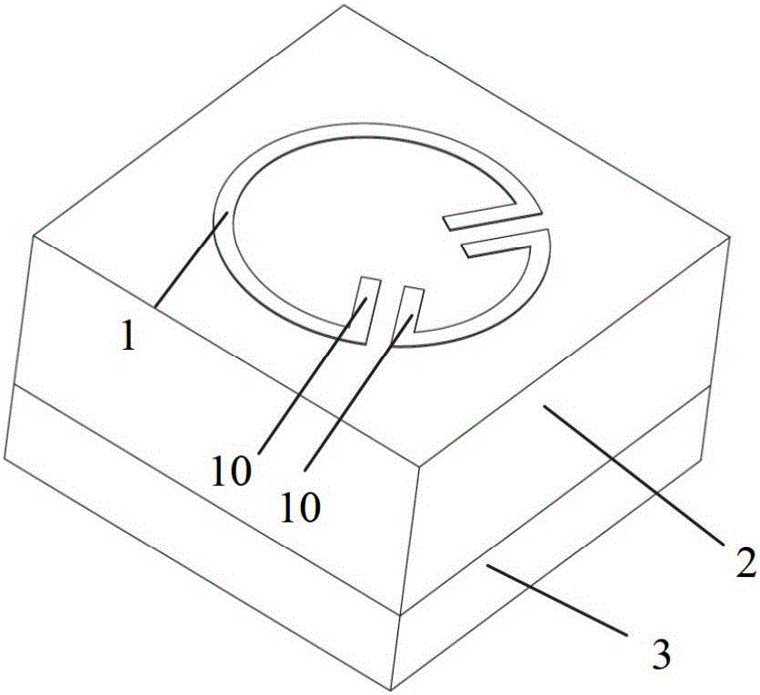
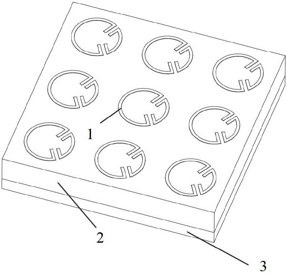
[0038] Such as figure 1 As shown, the absorbing metamaterial includes a magnetic electromagnetic absorbing material layer 2 and a conductive geometric structure unit 1 combined with the magnetic electromagnetic absorbing material layer 2 . The magnetic electromagnetic wave-absorbing material layer 2 can be based on rubber in combination with an electromagnetic wave absorber, and the electromagnetic wave absorber can be a particle ferrite or a micron / submicron metal particle absorber or a magnetic fiber absorber or a nano-magnetic absorber, which can pass The way of doping or proportioning is combined in the rubber matrix. The magnetic electromagnetic wave-absorbing material layer 2 may be a wave-absorbing patch material, which has a small thickness and can be produced automatically. The thickness and electromagnetic parameters of the magnetic electromagnetic wave-absorbing material layer 2 can be set according to the working frequency band of the wave-absorbing metamaterial, ...
Embodiment 2
[0043] This embodiment follows the component numbers and part of the content of the previous embodiments, wherein the same numbers are used to denote the same or similar components, and descriptions of the same technical content are selectively omitted. For the description of the omitted part, reference may be made to the foregoing embodiments, and this embodiment will not be repeated.
[0044] Such as Figure 5 As shown, the difference from Embodiment 1 is that the conductive geometric structure unit 4 is octagonal with openings, and parallel metal strips 40 are arranged at the openings. Such as Figure 5 As shown, the arrangement law of the conductive geometric structure unit 4 is a periodic law, and the periodic law is shown as a periodic arrangement in two directions perpendicular to each other in the plane, extending in the form of a square grid, but the arrangement law is not limited to this, and can be It is a misplaced arrangement or a disordered arrangement or an un...
Embodiment 3
[0048] This embodiment follows the component numbers and part of the content of the previous embodiments, wherein the same numbers are used to denote the same or similar components, and descriptions of the same technical content are selectively omitted. For the description of the omitted part, reference may be made to the foregoing embodiments, and this embodiment will not be repeated.
[0049] Such as Figure 8 As shown, the difference from Embodiment 1 is that the conductive geometric structure unit 5 is a quadrangle with an opening, and parallel metal strips 50 are arranged at the opening, and the center of the side where the opening is located is displaced into the quadrangle. Such as Figure 8 As shown, the arrangement law of the conductive geometric structure unit 5 is a periodic law, and the periodic law is shown as a periodic arrangement in two directions perpendicular to each other in the plane, extending in the form of a square grid, but the arrangement law is not l...
PUM
| Property | Measurement | Unit |
|---|---|---|
| Thickness | aaaaa | aaaaa |
Abstract
Description
Claims
Application Information


