
Method of making PCB dielectric layer

A production method and dielectric layer technology, applied in printed circuit manufacturing, electrical components, printed circuits, etc., can solve problems affecting signal transmission quality, different delays of signal lines, impedance differences, etc., to improve signal transmission quality and improve impedance control Accuracy, the effect of improving impedance fluctuation

Active Publication Date: 2016-07-20
GUANGZHOU FASTPRINT CIRCUIT TECH +2
View PDF3 Cites 6 Cited by
  • Summary
  • Abstract
  • Description
  • Claims
  • Application Information

AI Technical Summary

Problems solved by technology

When two or more impedance-controlled transmission lines are distributed at different positions on the substrate, the actual dielectric constants of their positions are different, which will lead to a large difference in the mutual impedance, so that different signal lines have different delays. Affects signal transmission quality
At the same time, due to the inconsistency of the dielectric constant at different positions on the same signal line, a certain section of the impedance value is large, and the other section of the impedance value is small, that is, impedance fluctuations occur, which leads to signal reflection and attenuation, resulting in signal transmission distortion.

Method used


Image

  • Method of making PCB dielectric layer
  • Method of making PCB dielectric layer
  • Method of making PCB dielectric layer

Examples


Embodiment example

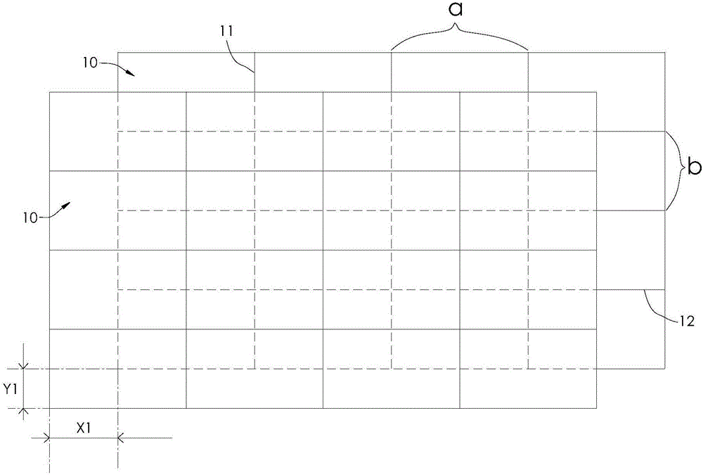
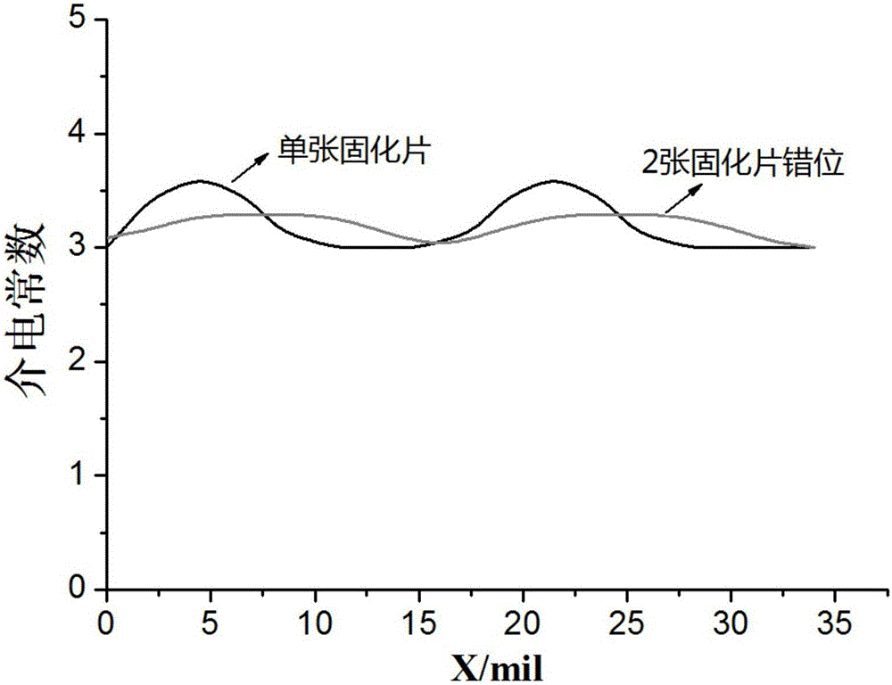
[0036] Such as figure 2 As shown, when making a PCB, one method uses a single prepreg 10 of model 1080 to make the PCB dielectric layer, and the other method uses two models of 1080 prepreg 10 to displace each other to make the PCB dielectric layer, and take X1 =0.5a, Y1=0.5b, as can be seen from the variation range of the two curves in the figure, the fluctuation range of the dielectric constant of the PCB dielectric layer made of two models of 1080 prepregs 10 is obviously small; figure 2 The middle abscissa is the distance from any point on the pre-assembled board to the origin, and the origin is figure 1 The endpoint in the lower left corner of the middle, the unit is mil; the ordinate is the dielectric constant, the unit is F / m.

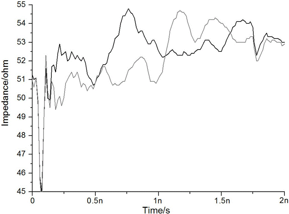
[0037] Such as image 3 As shown, when making the PCB dielectric layer, a piece of prepreg 10 with a model number of 1080 is used to make the PCB dielectric layer, and the impedance line is set along the X-axis direction, where the abscissa ...


PUM


Abstract

A method of making a PCB dielectric layer comprises the following steps: choosing two identical prepregs when making a dielectric layer of a multilayer printed circuit board; measuring the longitudinal glass fiber spacing a and the latitudinal glass fiber spacing b of the prepregs; completely overlapping the two identical prepregs, wherein, the longitudinal glass fiber bundles of the two prepregs extend along the X-axis direction, and the latitudinal glass fiber bundles of the two prepregs extend along the Y-axis direction; moving the lower prepreg along the X-axis direction and the Y-axis direction by X1 and Y1 respectively for dislocation, wherein X1 is non-integer times of a, and Y1 is non-integer times of b; pre-stacking the dislocated prepreg and a core board to get a pre-stacked board, coating the surface of the pre-stacked board with copper foil, placing the pre-stacked board on the chassis of a press, hot-pressing the pre-stacked board to form a multilayer board, and drilling, plating and etching the multilayer board to form an impedance controlled circuit. The uniformity of dielectric constant of the dielectric layer can be improved effectively.

Description

technical field [0001] The invention relates to a method for manufacturing a PCB dielectric layer. Background technique [0002] The base material (also known as the dielectric layer) of the printed circuit board is a copper-clad laminate, and the most commonly used FR4 copper-clad laminate is currently made of electronic glass fiber cloth as a reinforcing material. Treated glass fiber cloth, impregnated with resin glue, and then heat-treated (pre-baked) to make the thin sheet material made of resin is called prepreg. One or both sides of the prepreg are covered with copper foil of a certain thickness, and then heated. The sheet-like material formed by pressure treatment is FR4 copper clad laminate. Most of the prepregs used in the production of multilayer printed boards use E-glass fiber cloth (Electrical Glass, E-glass) as a reinforcing material, and E-glass is woven from glass fiber yarn. Due to the large difference in the dielectric constant of resin and glass fiber, t...

Claims


Application Information

Patent Timeline
IPC IPC(8): H05K3/00
CPCH05K3/0011H05K2203/068
Inventor 程柳军王红飞陈蓓
Owner GUANGZHOU FASTPRINT CIRCUIT TECH
Learn More