
Manufacturing method for groove grid power device and structure
A technology of power devices and manufacturing methods, which is applied in the manufacture of trench gate power devices and the field of trench gate power devices, can solve the problems of reducing on-resistance, etc., achieve reducing on-resistance, reducing unit size, and improving threshold voltage stability sexual effect
- Summary
- Abstract
- Description
- Claims
- Application Information
AI Technical Summary
Problems solved by technology
Method used
Image

Examples
Embodiment Construction
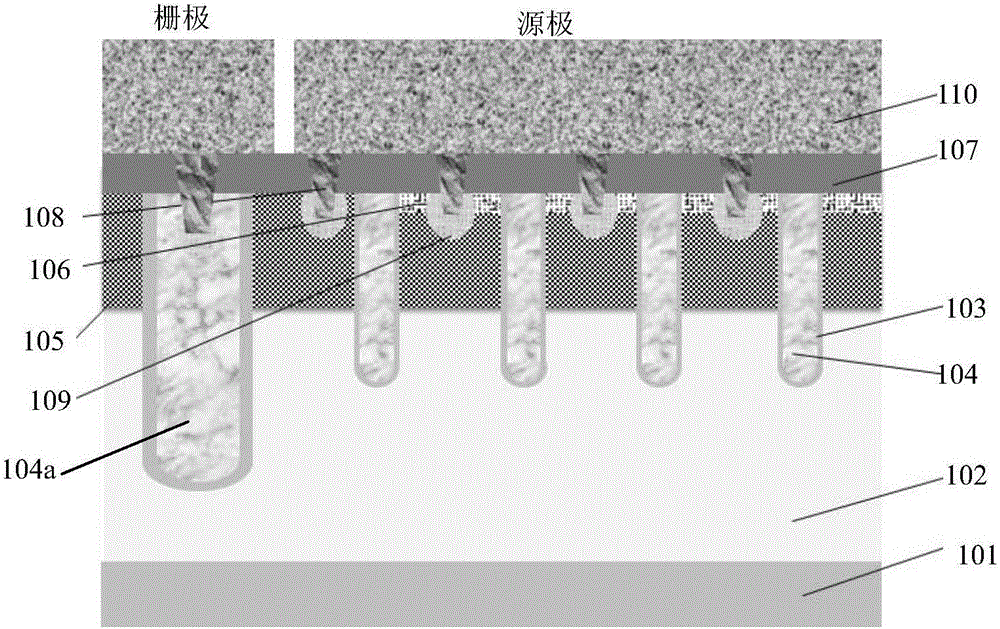
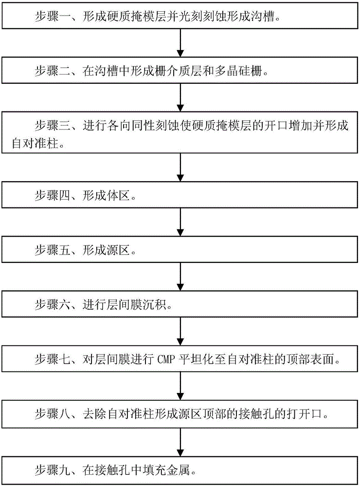
[0067] like figure 2 shown is a flow chart of a method for manufacturing a trench gate power device according to an embodiment of the present invention; such as 3A to 3O As shown, it is the device structure diagram of each step of the manufacturing method of the trench gate power device according to the embodiment of the present invention. In the method for manufacturing a trench gate power device according to the embodiment of the present invention, the conduction region of the trench gate power device is composed of a plurality of primitive cells arranged periodically, and the steps of forming each cell in the conduction region of the trench gate power device include:
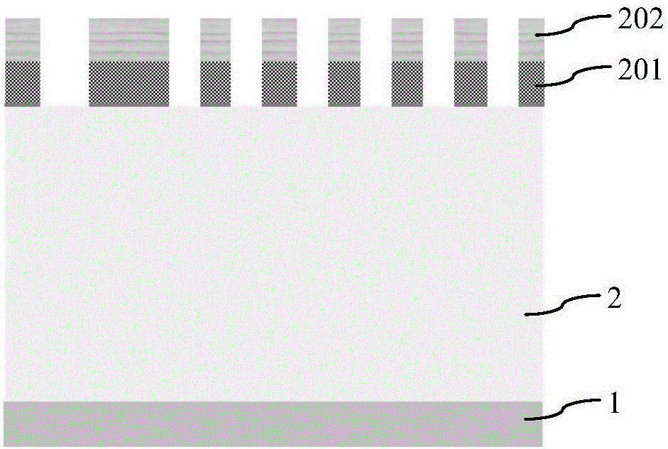
[0068] Step one, as Figure 3A As shown, a hard mask layer 201 is formed on the surface of the semiconductor substrate 1 of the first conductivity type; preferably, the semiconductor substrate 1 is a silicon substrate and a semiconductor epitaxial layer 2 of the first conductivity type is formed on the sur...
PUM
 Abstract
Description
Claims
Application Information