Optical film making method, optical device, display substrate and display device

A manufacturing method and technology of optical devices, applied in optical components, chemical instruments and methods, optics, etc., can solve the problems of large loss of light efficiency of OLED display devices, improve light output efficiency and spectral stability, eliminate micro-stress, Effect of Power Consumption Reduction

Active Publication Date: 2016-08-17
BOE TECH GRP CO LTD
View PDF5 Cites 8 Cited by
  • Summary
  • Abstract
  • Description
  • Claims
  • Application Information

AI Technical Summary

Problems solved by technology

[0004] However, due to the influence of the manufacturing process, there will be a microcavity structure between the film layer and the film layer and the substrate, which will cause a large loss of light efficiency of the OLED display device.

Method used


Image

  • Optical film making method, optical device, display substrate and display device
  • Optical film making method, optical device, display substrate and display device
  • Optical film making method, optical device, display substrate and display device

Examples


Embodiment 1

[0046] This embodiment provides a method for manufacturing an optical film, the optical film is used to refract light, and the method includes:

[0047] An uneven structure is formed on the surface of the optical film.

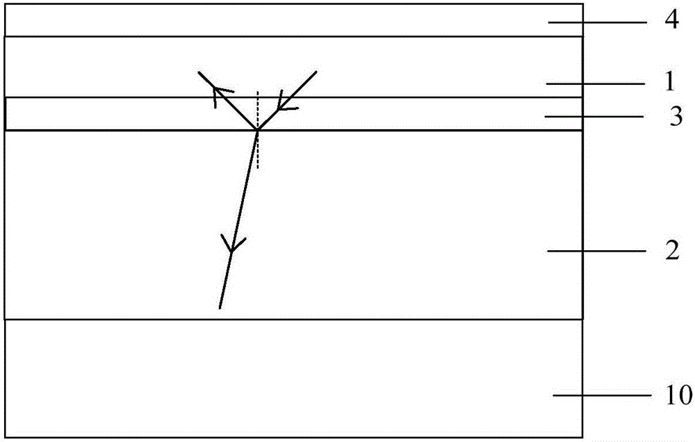
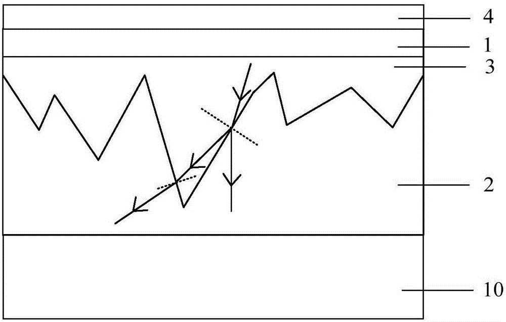
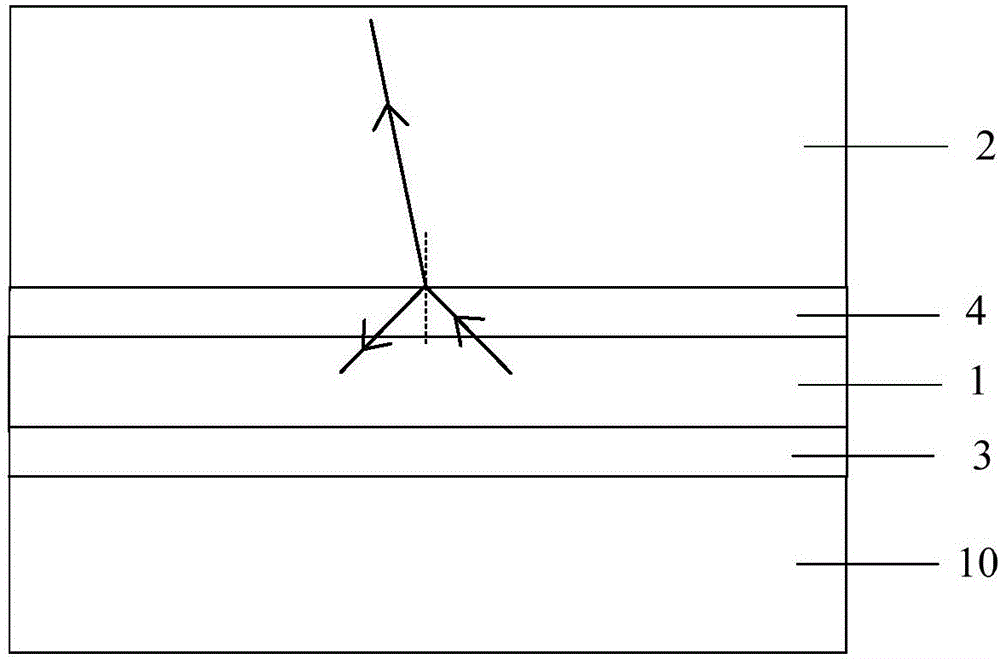
[0048] The optical film formed through the above steps has an uneven structure on its surface, which can improve the refraction of light, increase the transmittance and spectral stability of light, and refer to the specific principle figure 2 and Figure 4 As shown, the straight line with the arrow in the figure indicates the optical path. The protrusions and depressions of the uneven structure can change the optical path and increase the refraction effect. When applied to a display device, it can improve the display brightness of the product, reduce power consumption, and increase the viewing angle so that the display product is not affected by the viewing angle.

[0049] It should be noted that the surface of the film mentioned in this embodiment refers t...

Embodiment 2

[0087] Based on the same inventive concept, combining figure 1 and image 3 As shown, this embodiment provides an optical device, including a light-emitting device and an optical film 2 manufactured by the manufacturing method in Embodiment 1. The optical film 2 is used to refract the light emitted by the light-emitting device.

[0088] The above-mentioned optical device can refract light to the light-emitting side through the optical film, and can improve light output efficiency and spectral stability. When applied to a display device, it can also improve the display brightness of the product and reduce power consumption.

[0089] The light-emitting device may be a light-emitting device such as an organic light-emitting diode, a quantum dot light-emitting diode, or the like.

[0090] Taking an organic light emitting diode as an example, the light emitting device includes a light emitting layer 1 , an optical film 2 is closer to the light emitting side of the light emitting d...


PUM


Abstract

The invention relates to the technical field of display and discloses an optical film making method, an optical device, a display substrate and a display device. The display device comprises a light emitter and an optical film, wherein the optical film is used for refracting light emitted by the light emitter to the light outlet side, improving light output efficiency, optical spectrum stability and the display brightness of a product and reducing the power consumption. An uneven structure is formed on the surface of the optical film through multiple times of curing and a micro-molding process, the light refracting effect is improved, and micro-stress, micro-cracks, micro-peaks and other undesirable phenomena produced by the micro-molding process can be eliminated.

Description

technical field [0001] The invention relates to the field of display technology, in particular to a method for manufacturing an optical film, an optical device, a display substrate and a display device. Background technique [0002] Light-emitting diode (Organic Light-Emitting Device) display devices have the advantages of active light emission, good temperature characteristics, low power consumption, fast response, bendable, ultra-thin and low cost, and have been widely used in display devices. [0003] OLED display devices can be divided into three types according to the direction of light emission: bottom-emitting OLEDs, top-emitting OLEDs and double-sided emitting OLEDs. In bottom-emitting OLEDs, light is emitted from the backplane direction, in top-emitting OLEDs, light is emitted from the top of the device, and in double-emitting OLEDs, light is emitted from both the substrate and the top of the device. [0004] However, due to the influence of the manufacturing proce...

Claims


Application Information

Patent Timeline
Patent Type & Authority Applications(China)
IPC IPC(8): H01L51/56H01L51/52
CPCH10K50/858H10K71/00B32B17/00G02B3/0031G02B3/0056H10K50/85H10K50/84H10K50/80H10K50/87H10K50/805H10K50/856H10K71/821G02B3/00
Inventor 杨久霞徐文艳
Owner BOE TECH GRP CO LTD
Why Eureka
Try Eureka