Pixel circuit, driving method and display equipment

A pixel circuit and circuit technology, applied in static indicators, instruments, etc., can solve the problems of DC bias and easy aging

Active Publication Date: 2016-08-24
BOE TECH GRP CO LTD +1
View PDF5 Cites 23 Cited by
  • Summary
  • Abstract
  • Description
  • Claims
  • Application Information

AI Technical Summary

Problems solved by technology

[0004] Embodiments of the present invention provide a pixel circuit, a driving method, and a displa...

Method used


Image

  • Pixel circuit, driving method and display equipment
  • Pixel circuit, driving method and display equipment
  • Pixel circuit, driving method and display equipment

Examples


Embodiment 1

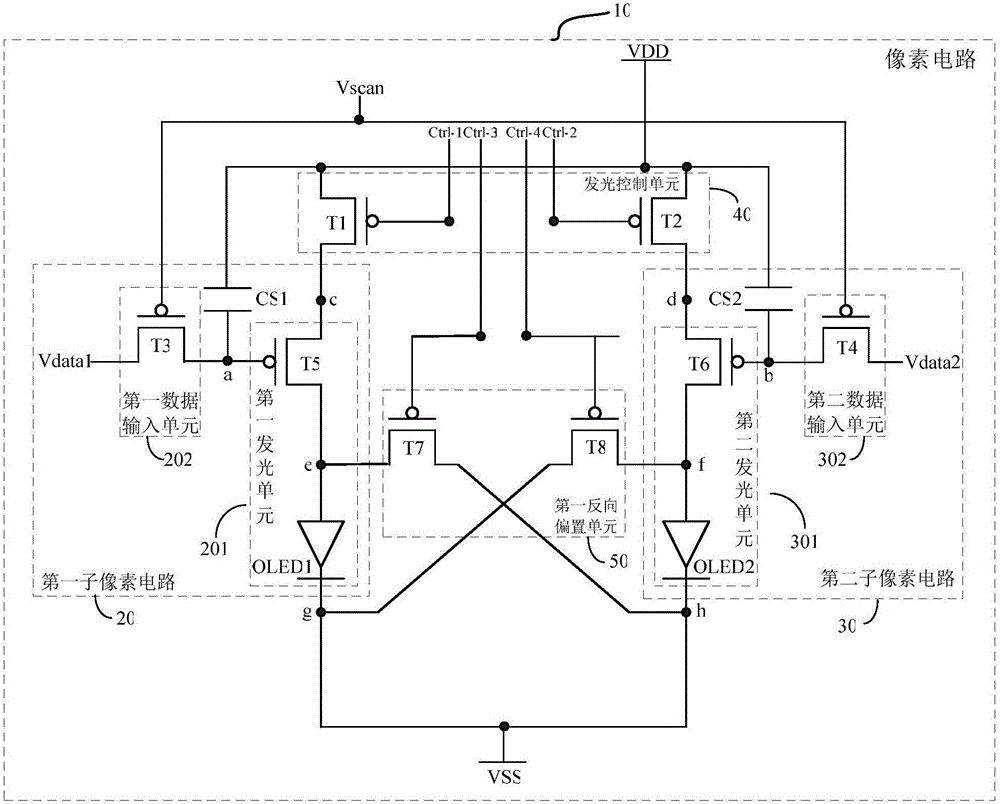
[0179] Embodiment one, with reference to figure 2 As shown, the embodiment of the present invention provides a pixel circuit 10, including: a first reverse bias unit 50, and adjacent first sub-pixel circuits 20 and second sub-pixel circuits 30, the first sub-pixel circuit 20 includes The first light emitting unit 201; the second sub-pixel circuit 30 includes a second light emitting unit 301; wherein, the first light emitting unit 201 is connected to the fifth node e and the seventh node g, and the second light emitting unit 301 is connected to the sixth node f and the eighth node Node h; the first reverse bias unit 50 is connected to the fifth node e, the sixth node f, the seventh node g, the eighth node h, the third control terminal Ctrl-3 and the fourth control terminal Ctrl-4;

[0180] The first light emitting unit 201 is used to emit light under the control of the first driving signal, and output the first driving signal to the fifth node e; the first reverse bias unit 50...

Embodiment 2

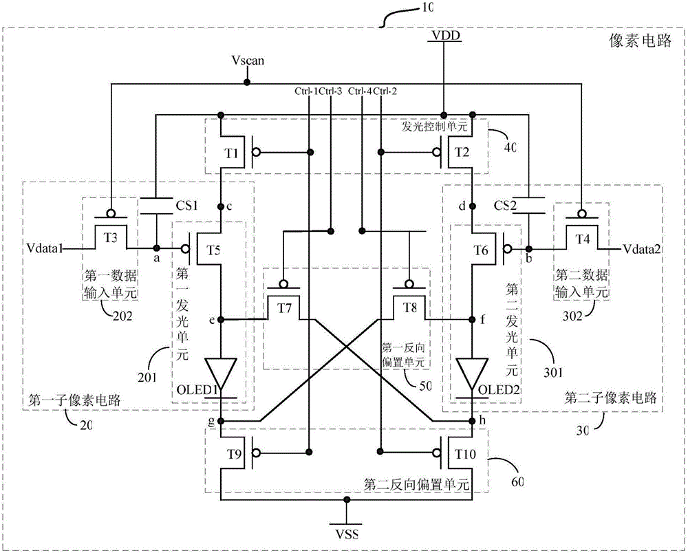
[0184] Embodiment two, refer to image 3 , Figure 4 , Figure 5 and Figure 6 As shown, the embodiment of the present invention provides a pixel circuit 10, and the specific implementation method is as follows:

[0185] Scenario 1, such as image 3 and Figure 5 The illustrated embodiment of the present invention provides a pixel circuit 10, wherein the first sub-pixel circuit 20 in the pixel circuit 10 further includes: a first data input unit 202, a first storage capacitor CS1;

[0186] The first data input unit 202 is connected to the first data terminal Vdata1, the first scanning terminal Vscan and the first node a; A data signal is output to the first node a;

[0187] The first storage capacitor CS1 is connected to the first node a and the first voltage terminal VDD, and the first storage capacitor CS1 is used to store a level between the first node a and the first voltage terminal VDD;

[0188] The first light emitting unit 201 is also connected to the first node...

Embodiment 3

[0236] Embodiment three, refer to image 3 , Figure 5 , Figure 7 , Figure 8 , Figure 9 , Figure 10 and Figure 11 As shown, the embodiment of the present invention provides a driving method of the pixel circuit 10,

[0237]Taking the first transistor T1, the second transistor T1, the third transistor T3, the fourth transistor T4, the fifth transistor T5, the sixth transistor T6, the seventh transistor T7 and the eighth transistor T8 in the pixel circuit 10 as transistors of the same type as Example: where all the transistors in the pixel circuit 10 are P-type transistors, the third control terminal Ctrl-3 and the fourth control terminal Ctrl-4 are connected to the same signal control line for illustration; the first time period t1 and the second time period Segment t2 together constitutes a frame of picture, and the time between t1 and t2 can be used to adjust the reverse bias time of the first light-emitting unit 201 and the second light-emitting unit 301. The timi...


PUM


Abstract

The invention provides a pixel circuit, a driving method and display equipment, and relates to the technical field of display, which solves the problem of easiness in aging of an OLED (organic light emitting diode) due to staying in direct current bias for a long time in the prior art. The pixel circuit comprises a first reverse bias unit, a first subpixel circuit and a second subpixel circuit, wherein the first subpixel circuit and the second subpixel circuit are adjacently arranged; the first subpixel circuit comprises a first light emitting unit; the second subpixel circuit comprises a second light emitting unit. The pixel unit provided by the embodiment is used for manufacturing OLED display equipment.

Description

technical field [0001] The present invention relates to the field of display technology, in particular to a pixel circuit, a driving method and a display device. Background technique [0002] Organic Light-Emitting Diode (full name in English: Organic Light-Emitting Diode, referred to as: OLED) display has the characteristics of light and thin, wide viewing angle, low power consumption, fast response, etc., so it has received extensive attention, and as a new generation of display methods, it has begun Gradually replace the traditional liquid crystal display (English full name: Liquid Crystal Display, abbreviation: LCD), and is widely used in mobile phone screens, computer monitors, full-color TVs, etc. According to different driving methods, OLEDs can be classified into passive matrix organic light emitting diodes (Passive matrix OLED, PMOLED for short) and active matrix organic light emitting diodes (Active-matrix OLED, AMOLED for short). [0003] Among them, the simplest...

Claims


Application Information

Patent Timeline
IPC IPC(8): G09G3/3291
CPCG09G3/3291G09G3/3233G09G2300/0443G09G2300/0804G09G2300/0819G09G2300/0852G09G2300/0861G09G2310/0256G09G2320/043G09G2330/028G09G2320/0233G09G2320/045G09G3/3225
Inventor 童振霄韦东梅
Owner BOE TECH GRP CO LTD
Why Eureka
Try Eureka