CMOS Transistor Junction Regions Formed By A CVD Etching And Deposition Sequence

A junction and crystalline technology, used in semiconductor devices, semiconductor/solid-state device manufacturing, electrical components, etc., can solve problems such as large diffusion resistance and insufficient optimization of diffusion resistance.

Active Publication Date: 2016-08-24
INTEL CORP
View PDF4 Cites 0 Cited by
  • Summary
  • Abstract
  • Description
  • Claims
  • Application Information

AI Technical Summary

Problems solved by technology

Narrow band of dopants can lead to large diffusion resistance and limit current flow from the channel to the silicide interface
In the replacement source-drain architecture of the current technology, the shape of the groove is better, but it is still not fully optimized in terms of diffusion resistance

Method used


Image

  • CMOS Transistor Junction Regions Formed By A CVD Etching And Deposition Sequence
  • CMOS Transistor Junction Regions Formed By A CVD Etching And Deposition Sequence
  • CMOS Transistor Junction Regions Formed By A CVD Etching And Deposition Sequence

Examples


Embodiment Construction

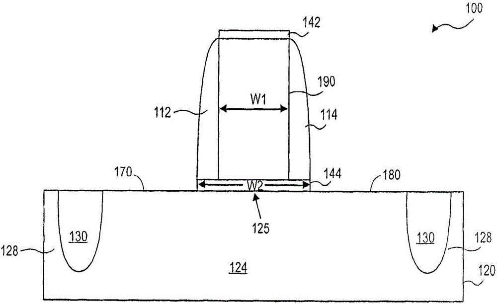
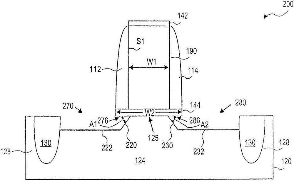
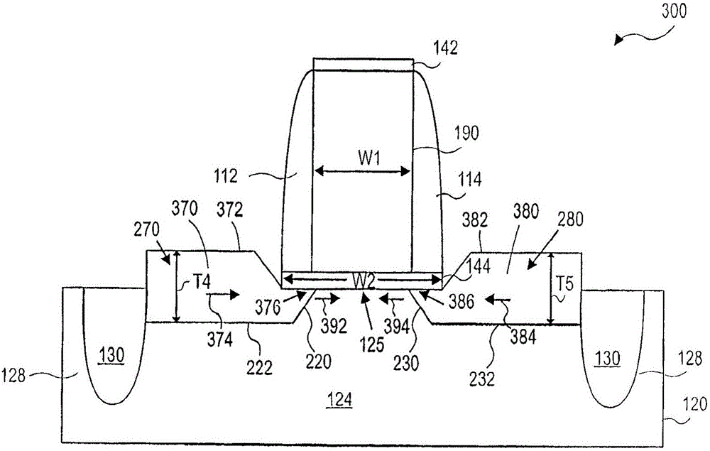
[0024] Locally strained transistor channel regions can be accomplished by forming source-drain regions in the channel region of a MOS transistor by selective epitaxy of a strain-generating material. Such a process flow may include etching substrate material in a source-drain region of a transistor in one process operation with an etch reactor. Subsequent operations may include replacing the removed material with Si alloy material in the deposition reactor. The etch reactor and the deposition reactor may be physically distinct and separate. Thus, before starting the Si alloy deposition process, the substrate must be removed from the etch reactor and exposed to atmospheric pressure. The above Si alloy can be pure Si or Si 1-x Ge x or Si 1-x C x , and can be undoped or doped with P-type or N-type dopants. The deposition process described above may be selective or non-selective. According to the examples presented herein, the etch reactor and the deposition reactor may be p...


PUM


Abstract

The invention adds to the art of replacement source-drain CMOS transistors. Processes may involve etching a recess in the substrate material using one equipment set, then performing deposition in another. Disclosed is a method to perform the etch and subsequent deposition in the same reactor without atmospheric exposure. In-situ etching of the source-drain recess for replacement source-drain applications provides several advantages over state of the art ex-situ etching. Transistor drive current is improved by: (1) Eliminating contamination of the silicon-epilayer interface when the as-etched surface is exposed to atmosphere and (2) Precise control over the shape of the etch recess. Deposition may be done by a variety of techniques including selective and non-selective methods. In the case of blanket deposition, a measure to avoid amorphous deposition in performance critical regions is also presented.

Description

[0001] The filing date of the parent application of this divisional application is January 4, 2006, the application number is 200680006549.5, and the title of the invention is "CMOS transistor junction region formed by CVD etching and deposition sequence". technical field [0002] The present invention relates to circuit devices and the manufacture and construction of circuit devices. Background technique [0003] Enhancement of the performance of circuit devices on a substrate (e.g., integrated circuit (IC) transistors, resistors, capacitors, etc.) on a semiconductor (e.g., silicon) substrate, typically during the design, manufacture, and operation of those devices major factor. For example, during the design and fabrication or formation of metal-oxide-semiconductor (MOS) transistor devices such as those used in complementary metal-oxide-semiconductor (CMOS), it is often necessary to increase the channel The movement of electrons in the channel, and the need to improve the...

Claims


Application Information

Patent Timeline
Patent Type & Authority Applications(China)
IPC IPC(8): H01L21/336H01L21/02
CPCH01L21/02381H01L21/02532H01L21/0262H01L21/02639H01L29/66628H01L29/7834H01L29/7848H01L29/517H01L21/2053H01L21/8238B82Y40/00H01L21/18H01L21/205H01L21/3065
Inventor A.墨菲G.格拉斯A.韦斯特迈尔M.哈滕多夫J.万克
Owner INTEL CORP
Why Eureka
Try Eureka